Low-power consumption semiconductor memory device

a memory device and low power consumption technology, applied in semiconductor devices, digital storage, instruments, etc., can solve the problems of reduced processing efficiency, misreading data, and disadvantageous increase of active standby current (iccb>3/b>)

Inactive Publication Date: 2005-02-24
RENESAS ELECTRONICS CORP
View PDF20 Cites 6 Cited by
  • Summary
  • Abstract
  • Description
  • Claims
  • Application Information

AI Technical Summary

Benefits of technology

It is an object of the present invention to provide a semiconductor memory device capable of being driven with a low voltage and having long refresh intervals.

Problems solved by technology

If the voltage at the storage node is further lowered from the precharge voltage Vccs / 2 after time Tref, the H data is determined to be L data, resulting in misreading of the data.
Therefore, a processor is kept in a waiting state, resulting in reduced processing efficiency.
As a result, the active standby current (Icc3) is disadvantageously increased.

Method used


Image

  • Low-power consumption semiconductor memory device
  • Low-power consumption semiconductor memory device
  • Low-power consumption semiconductor memory device

Examples


embodiment 1

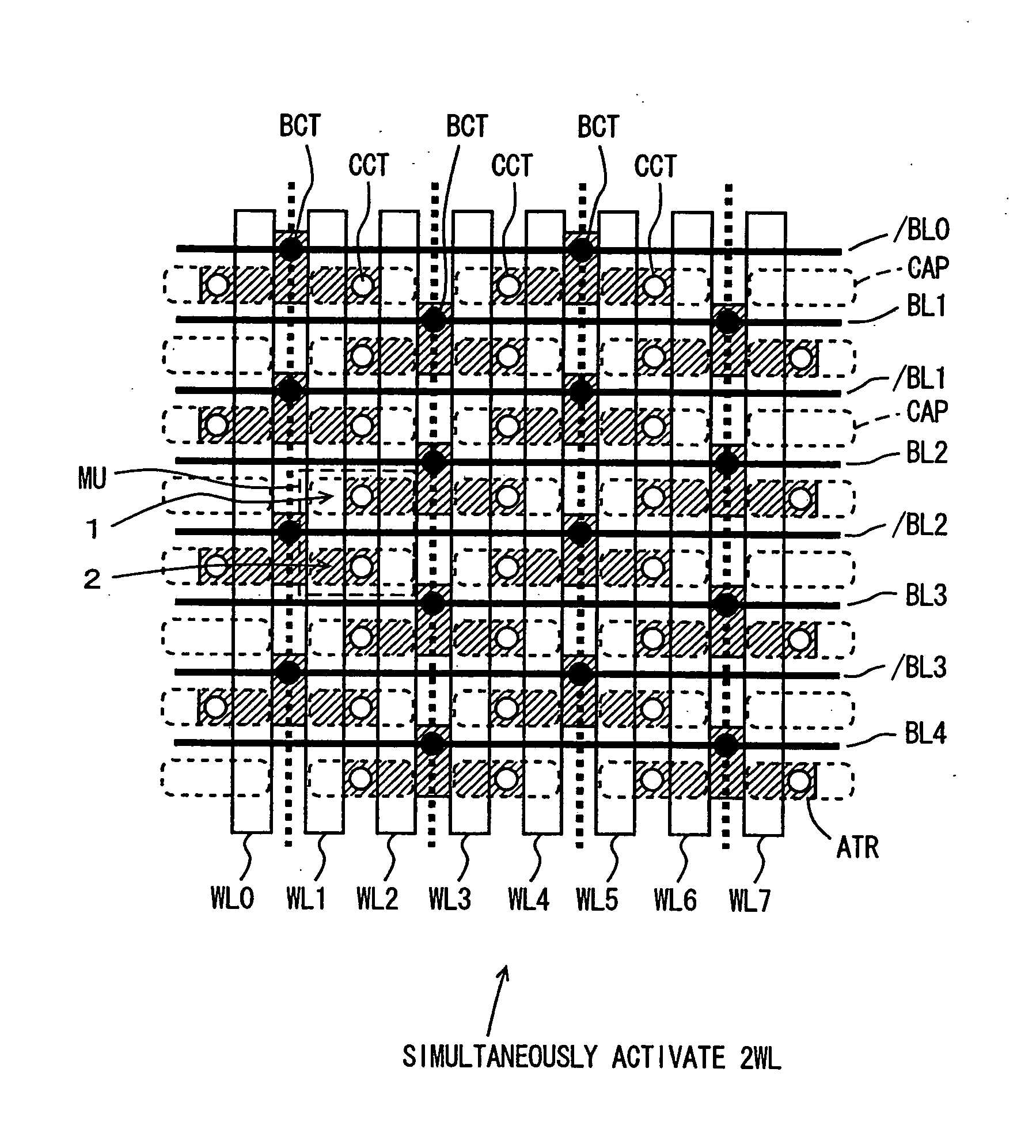
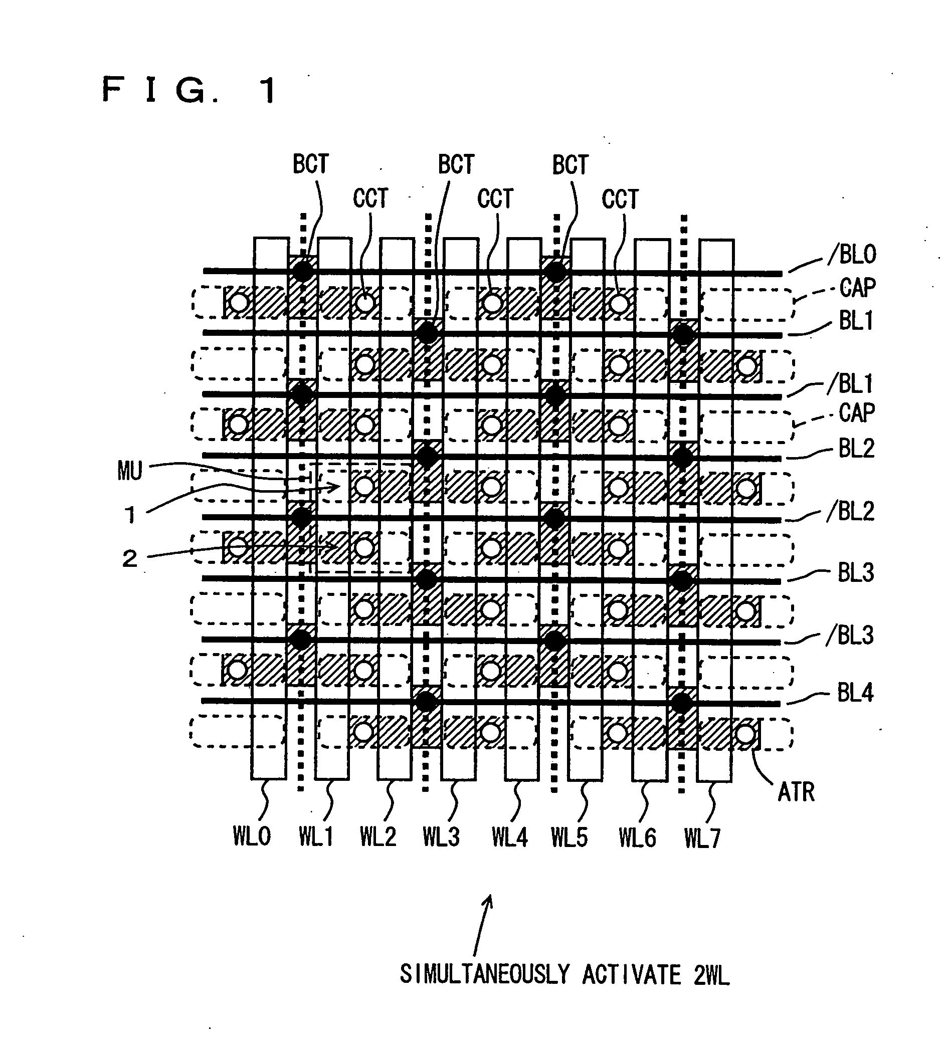
FIG. 1 is a diagram schematically showing the layout of an array portion of a semiconductor memory device according to Embodiment 1 of the present invention. In FIG. 1, reversed-T-shaped element active regions ATR are arranged in row and column directions. Element active regions ATR in adjacent columns are shifted from each other by two rows. Bit lines BL and / BL are provided for respective columns of the element active regions. FIG. 1 representatively shows bit lines / BL0, BL1, / BL1 . . . BL3, / BL3 and BL4. Each of bit lines BL1 to BL4 and / BL0 to / BL3 is coupled to element active region ATR of the corresponding column through a respective bit line contact BCT.

Memory cell capacitors CAP are provided on each element active region ATR so as to be opposite to each other with respect to a bit line contact BCT. These memory cell capacitors CAP are arranged being aligned in the row and column directions. Each memory cell capacitor CAP is coupled to the corresponding element active regi...

embodiment 2

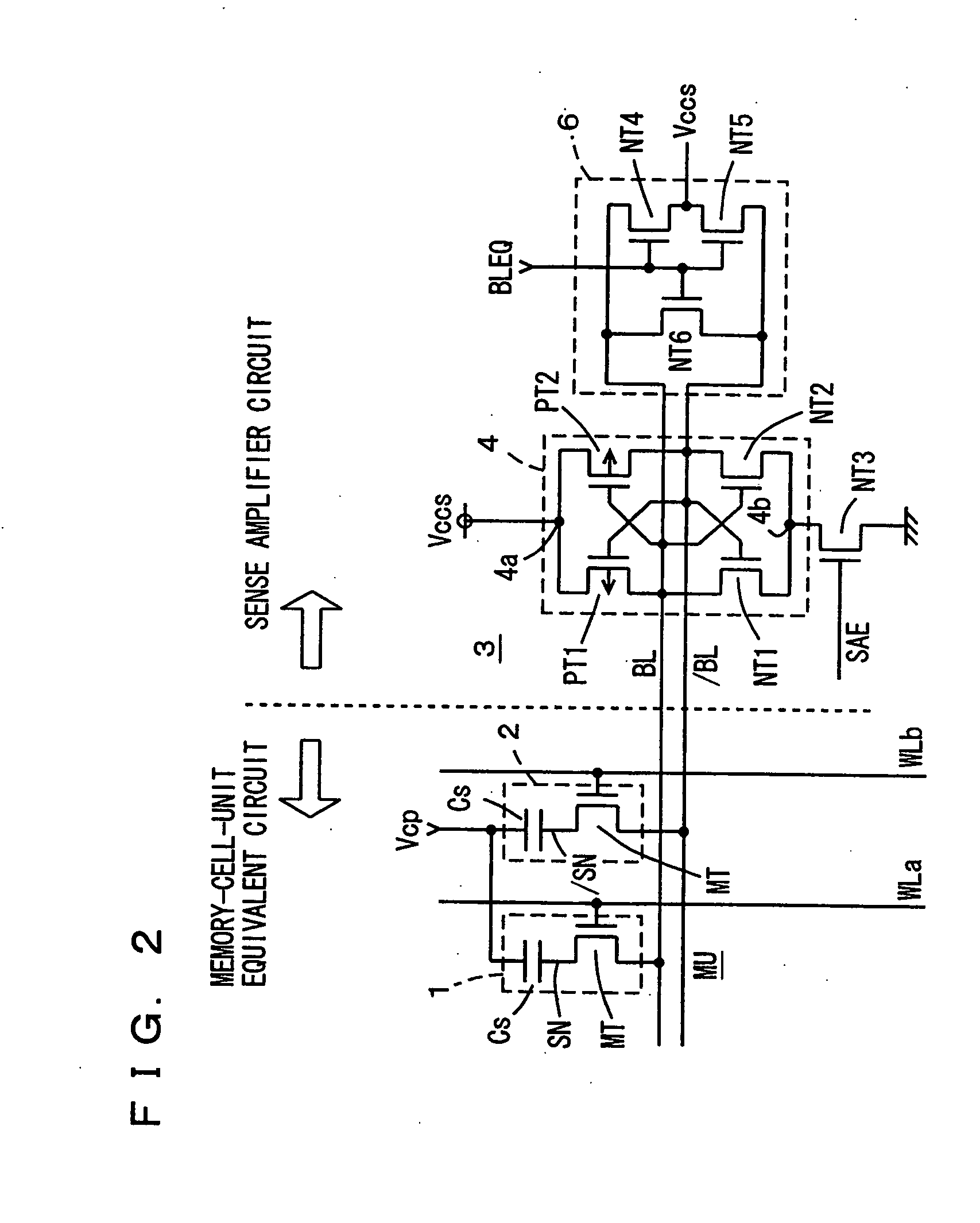
FIG. 10 is a diagram showing the structure of a main part of a semiconductor memory device according to Embodiment 2 of the present invention. FIG. 10 shows the structure of a portion associated with one memory unit MU. Like Embodiment 1, memory unit MU includes storage elements 1 and 2 each having an access transistor and a capacitor. A sense amplifier circuit 3 is provided for bit lines BL and / BL. Similarly to Embodiment 1, sense amplifier circuit 3 includes: a sense amplifier 4 including cross-coupled P-channel MOS transistors and cross-coupled N-channel MOS transistors; and a sense amplifier activation transistor NT3 for activating sense amplifier 4 in response to activation of a sense amplifier activation signal SAE.

A bit-line precharging / equalizing circuit 16 is provided in order to precharge bit lines BL and / BL to the sense power supply voltage Vccs level in the standby cycle. Bit-line precharging / equalizing circuit 16 includes: P-channel MOS transistors PT3 and PT4 rende...

embodiment 3

FIG. 14 is a diagram schematically showing the structure of a main part of a semiconductor memory device according to Embodiment 3 of the present invention. FIG. 14 shows the structure of a portion associated with one memory cell unit MU. In the structure of FIG. 14, bit-line precharging / equalizing circuit 6 transmits ground voltage GND onto bit lines BL and / BL instead of sense power supply voltage Vccs.

Bit lines BL and / BL are precharged to the ground voltage GND level. Therefore, in sense amplifier circuit 3, sense power supply node 4a of sense amplifier 4 is coupled to the sense power supply line through a sense amplifier activation transistor PT6 that is rendered conductive in response to a sense amplifier activation signal / SAE. Sense amplifier activation transistor PT6 is formed of a P-channel MOS transistor. Internal node 4b of sense amplifier 4 is coupled to the ground node. Bit-line precharging / equalizing circuit 6 has the same structure as that of Embodiment 1, and incl...


PUM


Abstract

A memory cell unit includes a first storage element and a second storage element for storing complementary data with each other. In a selected state, the first and second storage elements are connected to complementary bit lines, respectively at a time. In a standby state, the bit lines are precharged to a voltage (Vccs or GND) corresponding to the data stored in the memory cell unit. Refresh-free, low-current-consumption semiconductor memory device operating stably even under a low power supply voltage can be implemented.

Description

BACKGROUND OF THE INVENTION 1. Field of the Invention The present invention generally relates to a semiconductor memory device, and particularly to a dynamic semiconductor memory device with information stored in a capacitor. More particularly, the present invention relates to a dynamic semiconductor memory device suitable for integration into a system LSI (large scale integrated circuit) and operating under a low power supply voltage. 2. Description of the Background Art A dynamic random access memory (DRAM) is generally used in order to implement a mass storage memory in a system LSI with a memory and a logic integrated therein. The DRAM includes memory cells each formed of a single capacitor and a single transistor, and therefore, the memory cell occupies a small area. Moreover, the cost per bit is inexpensive. As a result, the DRAM can implement a mass storage memory with a small occupying area. FIG. 27 is a diagram schematically showing the structure of a main part of a con...

Claims


Application Information

Patent Timeline
Patent Type & Authority Applications(United States)
IPC IPC(8): G11C7/12G11C11/405G11C11/409G11C11/4094H01L21/8242H01L27/10H01L27/108
CPCG11C11/4094G11C7/12
Inventor FUJINO, TAKESHIARIMOTO, KAZUTAMISHIMANO, HIROKI
Owner RENESAS ELECTRONICS CORP
Why Eureka
Try Eureka