

Production method of sic monitor wafer
a production method and monitor technology, applied in the direction of crystal growth process, solid state diffusion coating, after-treatment details, etc., can solve the problems of impurities mixing in the grinding process, easy scratch damage on the wafer surface, and difficulty in producing ultra-flat surfaces
- Summary
- Abstract
- Description
- Claims
- Application Information
AI Technical Summary
Benefits of technology
Problems solved by technology
Method used
Image

Examples
Embodiment Construction
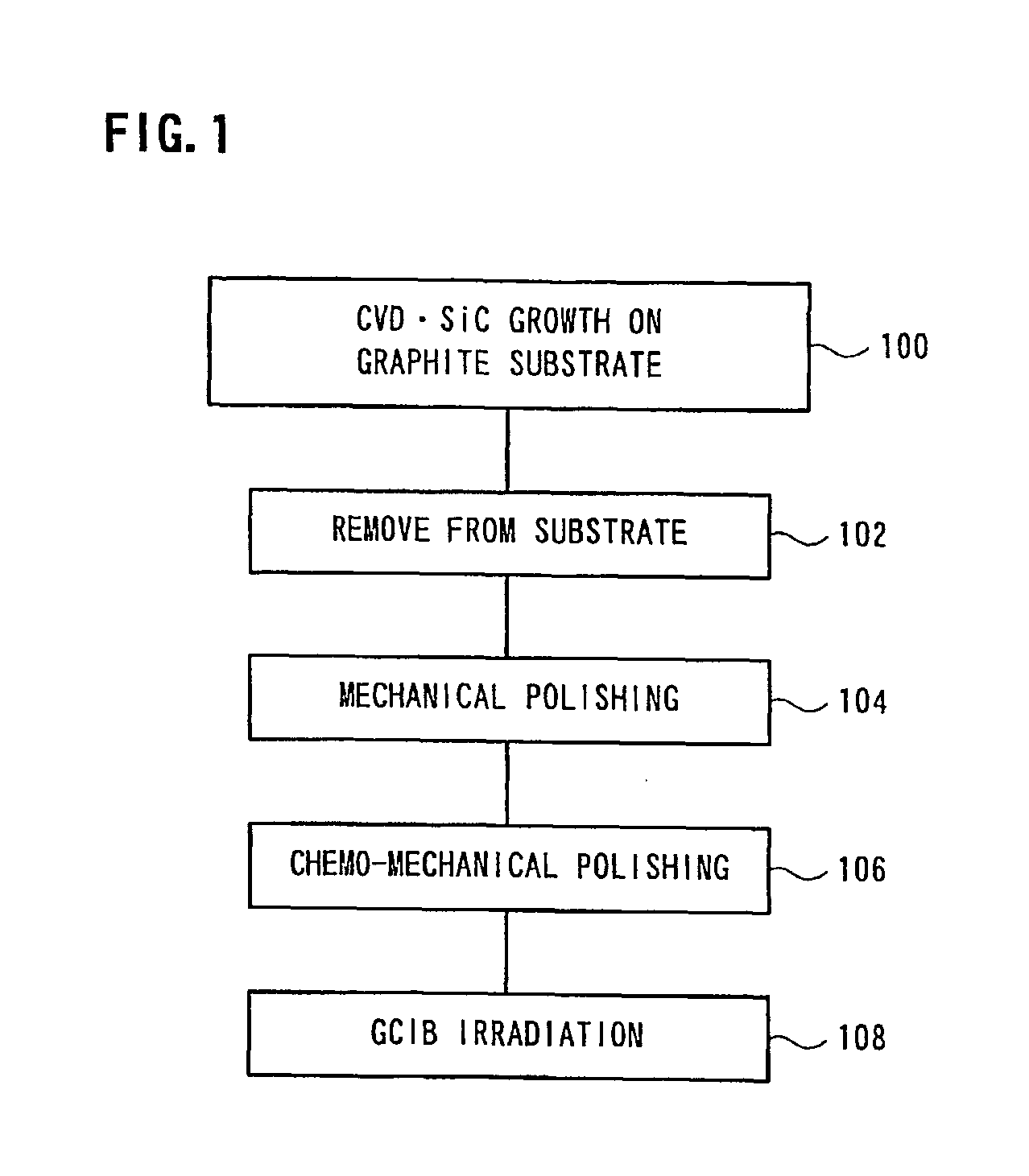
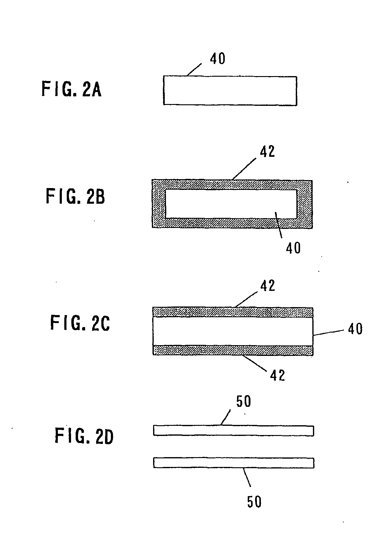
[0022] Hereinafter, a preferred embodiment of a production method of an SiC monitor wafer according to the present invention will be explained in detail with reference to the accompanying drawings.
[0023] As shown in FIG. 4, SiC is a substitutional type of diamond in its crystal structure and has a structure in which carbon atoms C and silicon atoms Si form a hexagonal lattice and a layer in which carbon atoms C are arranged and a layer in which silicon atoms Si are arranged are alternately placed along a direction of [111] axis. The bonding force between the layer in which the carbon atoms C are arranged and the layer in which the silicon atoms Si are arranged is weaker than a bonding force of the other parts, and therefore they tend to be cut in a direction parallel to a (111) surface. Therefore, SiC is easily cut in a direction parallel to the (111) surface as a border of the layer of the carbon atoms C and the layer of the silicon atoms Si, and the layer of carbon atoms C and th...
PUM
| Property | Measurement | Unit |
|---|---|---|
| Electric charge | aaaaa | aaaaa |
| Surface roughness | aaaaa | aaaaa |
| Surface roughness | aaaaa | aaaaa |
Abstract
Description
Claims
Application Information