
Composite laminate circuit structure

a circuit structure and laminate technology, applied in the field of laminate circuit structures, can solve the problems of exacerbated all the problems associated with additional thickness, difficult methods to be practiced,

Inactive Publication Date: 2005-03-03
INT BUSINESS MASCH CORP
View PDF16 Cites 6 Cited by
  • Summary
  • Abstract
  • Description
  • Claims
  • Application Information

AI Technical Summary

Benefits of technology

The present invention provides a way to make circuit structures for printed circuit boards that are thinner and can have higher density components without adding extra steps in the process. The invention also allows for easier customization of power planes and the ability to use advanced interconnection methods. The invention includes new ways to bond together subassemblies using dielectric materials and interposers, and a new method for making electrical interconnections between vias. The invention also provides new ways to make the dielectric materials used in the circuit structures, such as thermosetting resins and thermoplastic resins. Overall, the invention simplifies the process for creating complex circuit structures and expands the possibilities for designing custom power planes.

Problems solved by technology

These methods are difficult to practice due to the problems associated with handling bare copper.
These additional sticker sheets contribute additional thickness and exacerbate all the problems associated with additional thickness.

Method used


Image

  • Composite laminate circuit structure
  • Composite laminate circuit structure
  • Composite laminate circuit structure

Examples


Embodiment Construction

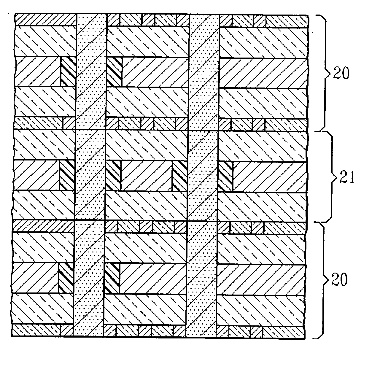
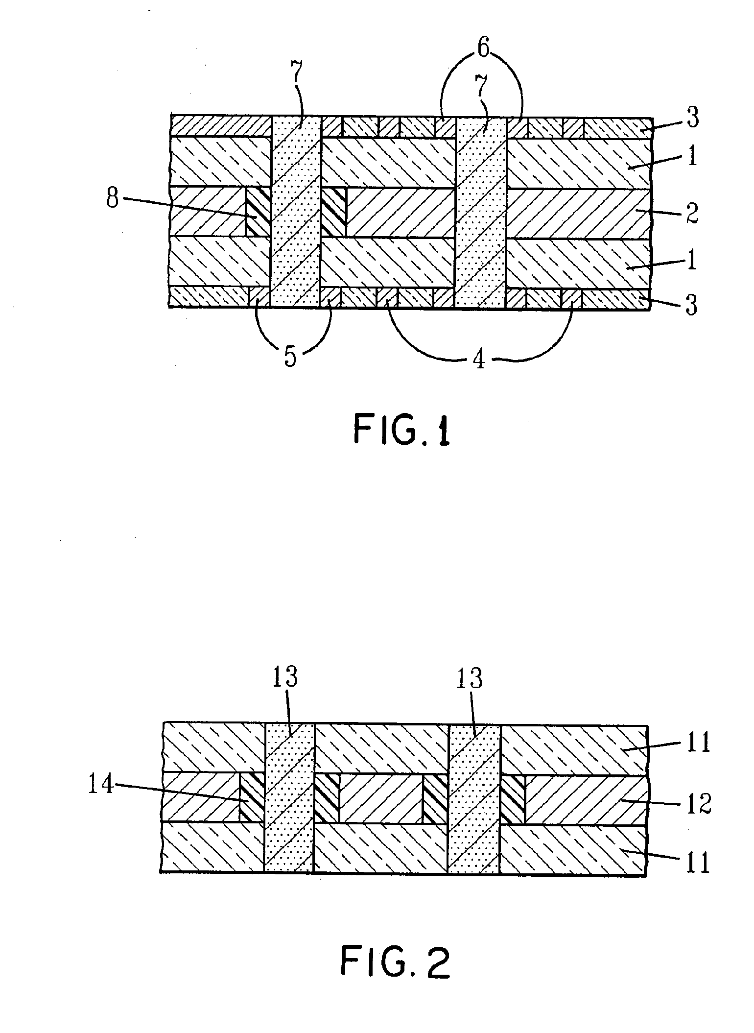
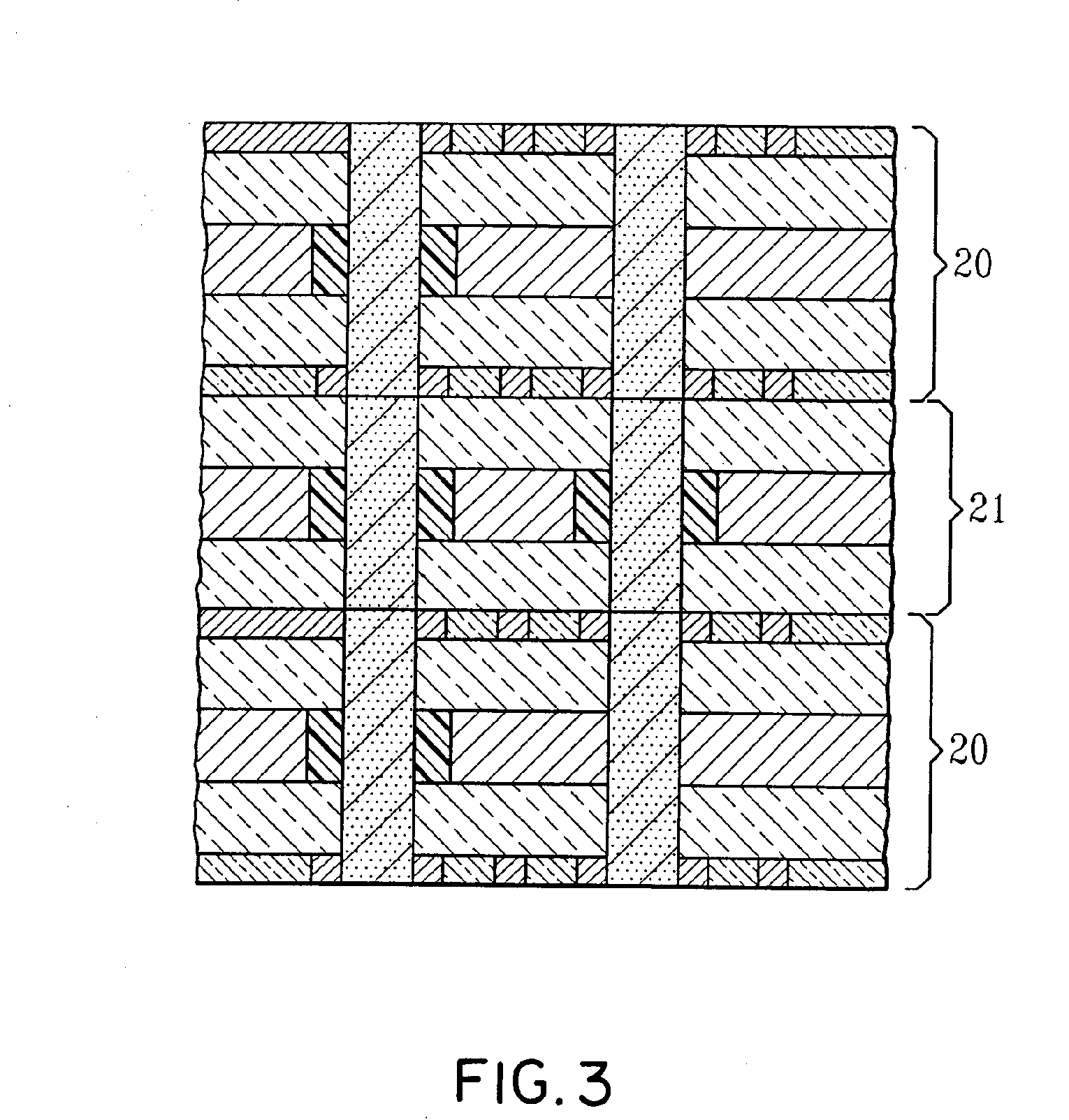
[0028] In order to facilitate an understanding of the present invention, reference will be made to the figures wherein the same numerals in different figures refer to the same or corresponding structures. Also in order to facilitate an understanding of the present invention, reference will be made to structures from 2S1P (2 signal plane-1 power plane) and 0S1P (0 signal plane-1 power plane) components.

[0029] Typically, the primary technique for fabricating the above subassembly components comprises applying a sheet of resin, (carried either on copper foil or, on an organic, peelable carrier film such as polyester), to either one or both sides of a 1 oz. or 0.5 oz. double treated copper sheet. During application the resin may or may not be fully cured.

[0030] Process flows to fabricate 2S1P and 0S1P subassemblies, covering a number of variations dependent on whether the power plane patterns are to be personalized by etching or drilling, and whether or not they will contain vias will...


PUM

PropertyMeasurementUnit
thickaaaaaaaaaa
thicknessaaaaaaaaaa
thickaaaaaaaaaa

Abstract

A laminate circuit structure assembly is provided that comprises at least two modularized circuitized voltage plane subassemblies; optionally an interposer located between each of the subassemblies, and wherein the subassemblies and interposer, if present, are bonded together with a cured dielectric coating. The interposer comprises dielectric layers disposed about an internal electrically conductive layer.

Description

CROSS REFERENCE TO RELATED APPLICATIONS [0001] This Application is a Division of application Ser. No. 09 / 625,135 filed on Jul. 25, 2000, the entire contents of which are incorporated herein by reference.TECHNICAL FIELD [0002] The present invention relates to laminate circuit structures, and more particularly to composite laminate circuit structures constructed from a plurality of modularized circuitized voltage plane subassemblies bonded together. The present invention also relates to a method for fabricating the laminate circuit structures. The present invention provides for planar, fine line external circuit flat lines and does not require an additional adhesive sheet nor glass cloth reinforcement. BACKGROUND OF INVENTION [0003] A conventional technique of forming a laminate circuit board structures includes forming layers of dielectric material and electrically conducting material to provide multiple layers of circuits and voltage planes. Voltage planes can be either ground plane...

Claims


Application Information

Patent Timeline
Patent Type & Authority Applications(United States)
IPC IPC(8): H05K3/40H05K3/44H05K3/46
CPCH05K3/4069H05K3/445H05K3/4614H05K3/4641H05K2201/09536Y10T29/49128H05K2201/09881H05K2201/10378Y10T29/49165Y10T29/49126H05K2201/096
Inventor JAPP, ROBERT M.KEVERN, GREGORY A.RUDIK, WILLIAM J.
Owner INT BUSINESS MASCH CORP
Learn More