Purification of silicon-containing materials

a technology of silicon-containing materials and purification methods, applied in the direction of silicon compounds, halogenated silanes, chemistry apparatus and processes, etc., can solve the problems of increasing the dielectric constant value of the deposited film, metal and organic impurities are fatal to the thin film, and the general acceptance of semiconductor processing applications

Inactive Publication Date: 2005-03-10
XU MINDI +2
View PDF9 Cites 45 Cited by
  • Summary
  • Abstract
  • Description
  • Claims
  • Application Information

AI Technical Summary

Benefits of technology

[0015] It is another object of the present invention to prevent the incorporation of additional impurities into the silicon-containing material while the material is being purified.

Problems solved by technology

While the above-referenced silicon-containing materials are commercially available, they are generally in an unacceptable condition for semiconductor processing applications.
These metal and organic impurities are fatal to the thin film in terms of the film quality and dielectric constant value.
For example, metal impurities will significantly increase the dielectric constant value of the deposited film and, even worse, will shorten adjacent layers of the chips.
While this method is effective for purifying methylsilane, it is ineffective for purifying low-k silicon-containing materials such as trimethylsilane, tetramethylsilane, dimethyldimethoxysilane, tetramethylcyclotetrasiloxane, octamethylcyclotetrasiloxane, dimethylphenyl silane, and dimethyldivinyl silane.
In particular, due to their physiochemical properties, these materials will quickly saturate the adsorbent material disclosed in Helly et al., thus rendering the purification process ineffective.
In U.S. Pat. No. 5,493,043 to Marko, a method is described in which an alumina bed is provided for removing impurities including olefins and chlorocarbons from a methylsilane mixture at a controlled temperature greater than about 150° C. While effective in removing impurities from methylsilane, this method would be rather costly when utilized with low-k silicon-containing materials, in particular materials that exist in liquid state at ambient temperature and pressure conditions, such as trimethylsilane, tetramethylsilane, dimethyldimethoxysilane, tetramethylcyclotetrasiloxane, octamethylcyclotetrasiloxane, dimethylphenyl silane, and dimethyldivinyl silane.
While these purifiers are effective in purifying trimethylsilane gas, they are not effective for certain low-k silicon-containing materials in liquid form, because these materials will react with the reactive metal hydride to produce a hydrogen by-product, thus creating an undesirable impurity during the purification process.
The carbon bed of Wikman et al. may not be useful for purifying low-k silicon-containing materials, especially liquid silicon-containing materials at ambient temperatures and pressures, since the low-k silicon-containing materials will likely be adsorbed with other organic impurities into the carbon, thus making the adsorption separation ineffective.

Method used


Image

  • Purification of silicon-containing materials
  • Purification of silicon-containing materials
  • Purification of silicon-containing materials

Examples


example 1

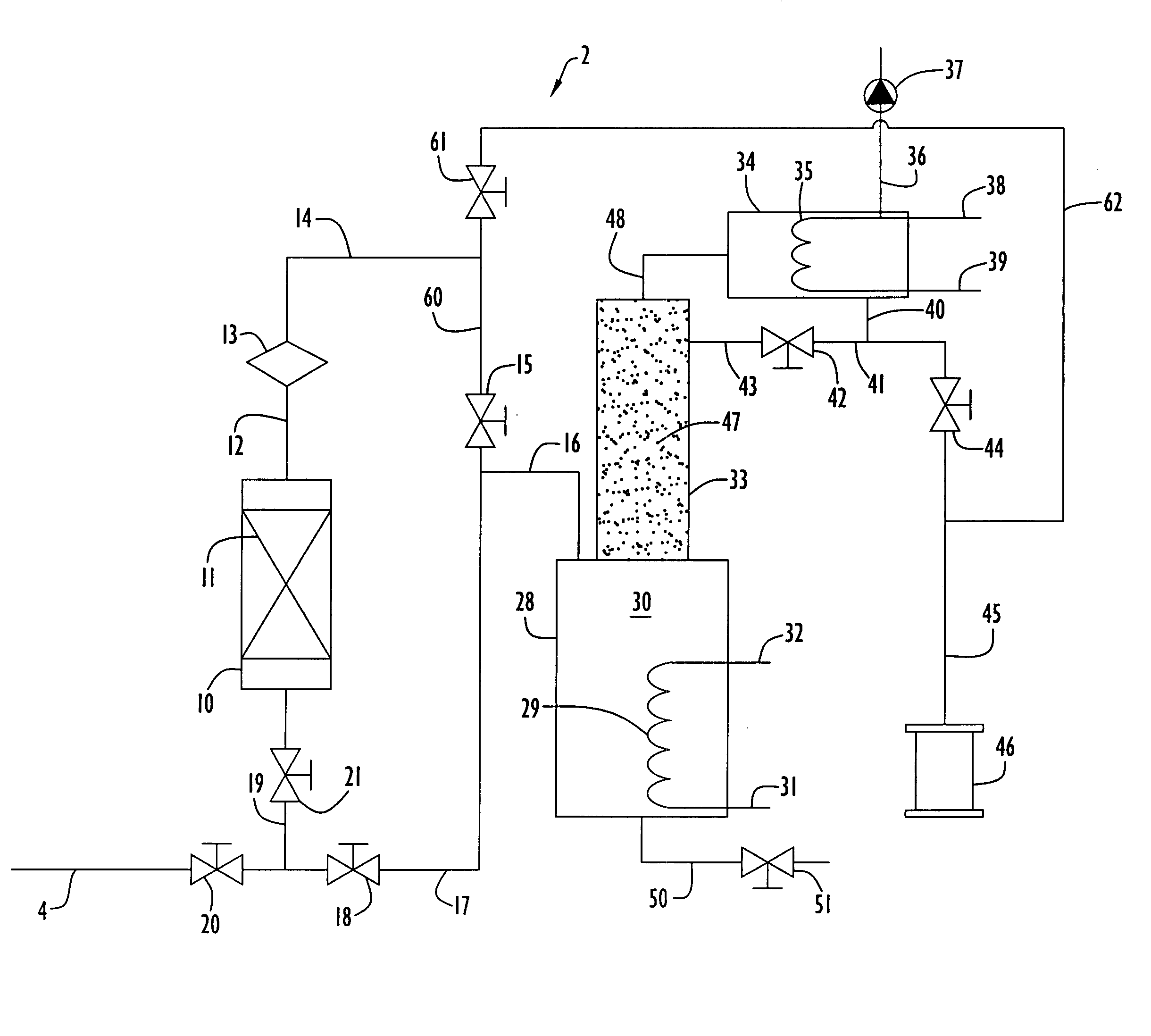
[0070] An adsorption unit was assembled utilizing a column of 2.54 centimeter (1 inch) inner diameter and 36.8 centimeters (14.5 inches) in length was packed with about 80 grams of Ambersorb® 563 adsorbent material for removing organic impurities from tetramethyl silane. Liquid tetramethyl silane flowed as influent upward through the column at a flow rate of about 20 milliliters / minute. The concentrations of tetrahydrofuran and toluene in the influent tetramethyl silane were spiked to 24,000 ppm (weight) and 4,570 ppm (weight), respectively. The adsorption unit was operated at ambient conditions of 24° C. and 270 kPa.

[0071] The concentrations of the tetrahydrofuran and toluene were measured periodically in the effluent stream from the adsorption unit utilizing a Varian model CP-3800 gas chromatograph having a detection limit of 150 ppb. The adsorption unit removed these impurities to sufficient levels that were below the detection limit of the gas chromatograph, indicating that the...

example 2

[0073] The adsorption unit of the previous example was regenerated after its saturation by heating the unit to a temperature about 200° C. while purging the unit with nitrogen gas at a flow rate of 3 liters / minute for a period of six hours. After this purging process, the material stream spiked with impurities as described in the previous example was flowed through the unit, and the unit was determined to be fully regenerated and performed in the same manner as described in the previous example prior to saturation of the adsorbent material.

example 3

[0074] The process as described in Example 1 was performed in the same manner as the present example, with the exception that the adsorption unit was packed with activated carbon grains instead of Ambersorb®563 adsorbent material and the concentrations of tetrahydrofuran and toluene in the influent tetramethyl silane were spiked to 5,048 ppm (weight) and 4 ppm (weight) respectively. The influent stream was directed through the column as the same flow rate as described in Example 1, and impurity levels of toluene and tetrahydrofuran in the effluent were not detected for a period of 30 minutes. At the point in time when the gas chromatograph began detecting impurity concentrations, the process was halted and the amount of impurities within the adsorbent material was measured. It was determined that at least 2.8 grams of tetrahydrofuran and at least 2.06 milligrams of toluene were adsorbed in the activated carbon grains and were thus removed from the tetramethyl silane during the proce...


PUM

PropertyMeasurementUnit
dielectric constantaaaaaaaaaa
temperatureaaaaaaaaaa

Abstract

Systems and methods of purifying a silicon-containing material include the step of directing the silicon-containing material in a liquid state through an adsorption unit including an adsorbent material to facilitate adsorption of at least one component from the silicon-containing material. Alternatively, the silicon-containing material is directed, in liquid state and/or gaseous state, through two or more purification units, including an adsorption unit, a vaporization unit, a filter unit and a condenser. The silicon-containing material can be a low-k silicon-containing material such as trimethylsilane, tetramethylsilane, dimethyldimethoxysilane, tetramethylcyclotetrasiloxane, octamethylcyclotetrasiloxane, dimethylphenyl silane, and dimethyldivinyl silane.

Description

CROSS-REFERENCE TO RELATED APPLICATIONS [0001] This application claims priority from U.S. Provisional Patent Application Ser. No. 60 / 500,214, entitled “Method for Purification of Organosilicate Compounds”, and filed Sep. 4, 2003. The disclosure of this provisional patent application is incorporated herein by reference in its entirety.BACKGROUND OF INVENTION [0002] 1. Field of Invention [0003] The present invention pertains to methods and systems for purifying silicon-containing compounds for use in semiconductor manufacturing processes. [0004] 2. Related Art [0005] As the size of integrated circuit chips decreases, semiconductor manufacturers are searching for viable materials to deposit thin films with lower dielectric constant (low-k) values of the interconnect system. A low dielectric constant is critical to advanced semiconductor manufacturing because it allows metal lines to be packed closer together on a chip with less risk of electrical signal leakage between adjacent layers....

Claims


Application Information

Patent Timeline
Patent Type & Authority Applications(United States)
IPC IPC(8): C01B33/107C07F7/20
CPCC07F7/20C01B33/10784
Inventor XU, MINDISAYASANE, TAYGIRARD, JEAN-MARC
Owner XU MINDI
Why Eureka
Try Eureka