At-speed ATPG testing and apparatus for SoC designs having multiple clock domain using a VLCT test platform

a clock domain and test platform technology, applied in the direction of electronic circuit testing, measurement devices, instruments, etc., can solve the problems affecting the overall test cost, and achieve the effect of enhancing simplicity and saving additional costs

Active Publication Date: 2005-03-10
TEXAS INSTR INC
View PDF10 Cites 79 Cited by
  • Summary
  • Abstract
  • Description
  • Claims
  • Application Information

AI Technical Summary

Benefits of technology

[0016] Advantages of this design include but are not limited to an integrated circuit chip or SoC design that is VLCT compliant which impacts the overall test cost. Since the number of transition fault patterns is large, this feature provides additional savings. This design supports pure at-speed transition fault testing using scan justified or functionally justi

Problems solved by technology

Advantages of this design include but are not limited to an integrated circuit

Method used


Image

  • At-speed ATPG testing and apparatus for SoC designs having multiple clock domain using a VLCT test platform
  • At-speed ATPG testing and apparatus for SoC designs having multiple clock domain using a VLCT test platform
  • At-speed ATPG testing and apparatus for SoC designs having multiple clock domain using a VLCT test platform

Examples


Embodiment Construction

[0028] The present invention will now be described more fully hereinafter with reference to the accompanying drawings, in which embodiments of the invention are shown. This invention may, however, be embodied in many different forms and should not be construed as limited to the embodiments set for the herein. Rather, these embodiments are provided so that this disclosure will be thorough and complete, and will fully convey the scope of the invention to those skilled in the art.

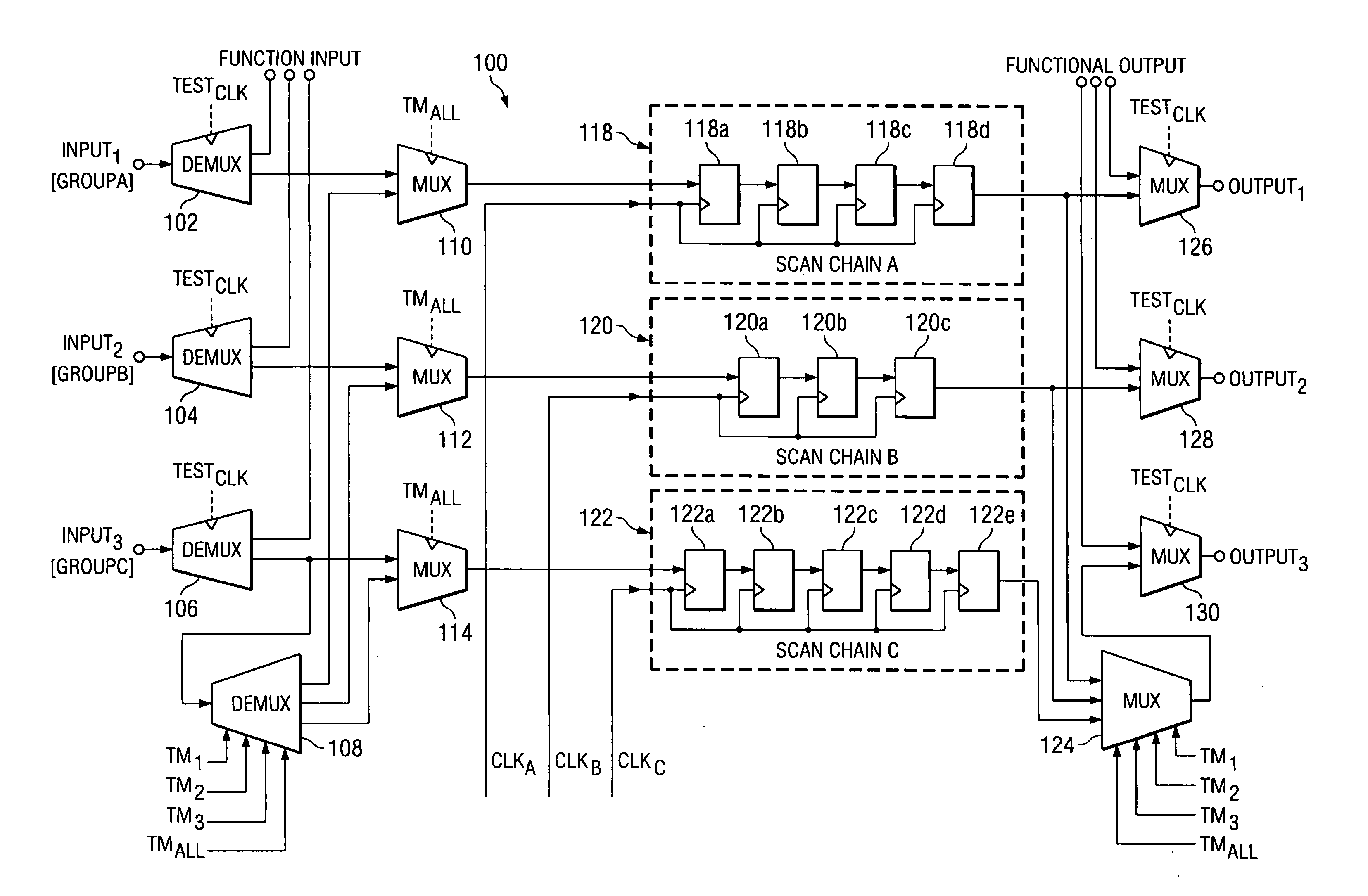
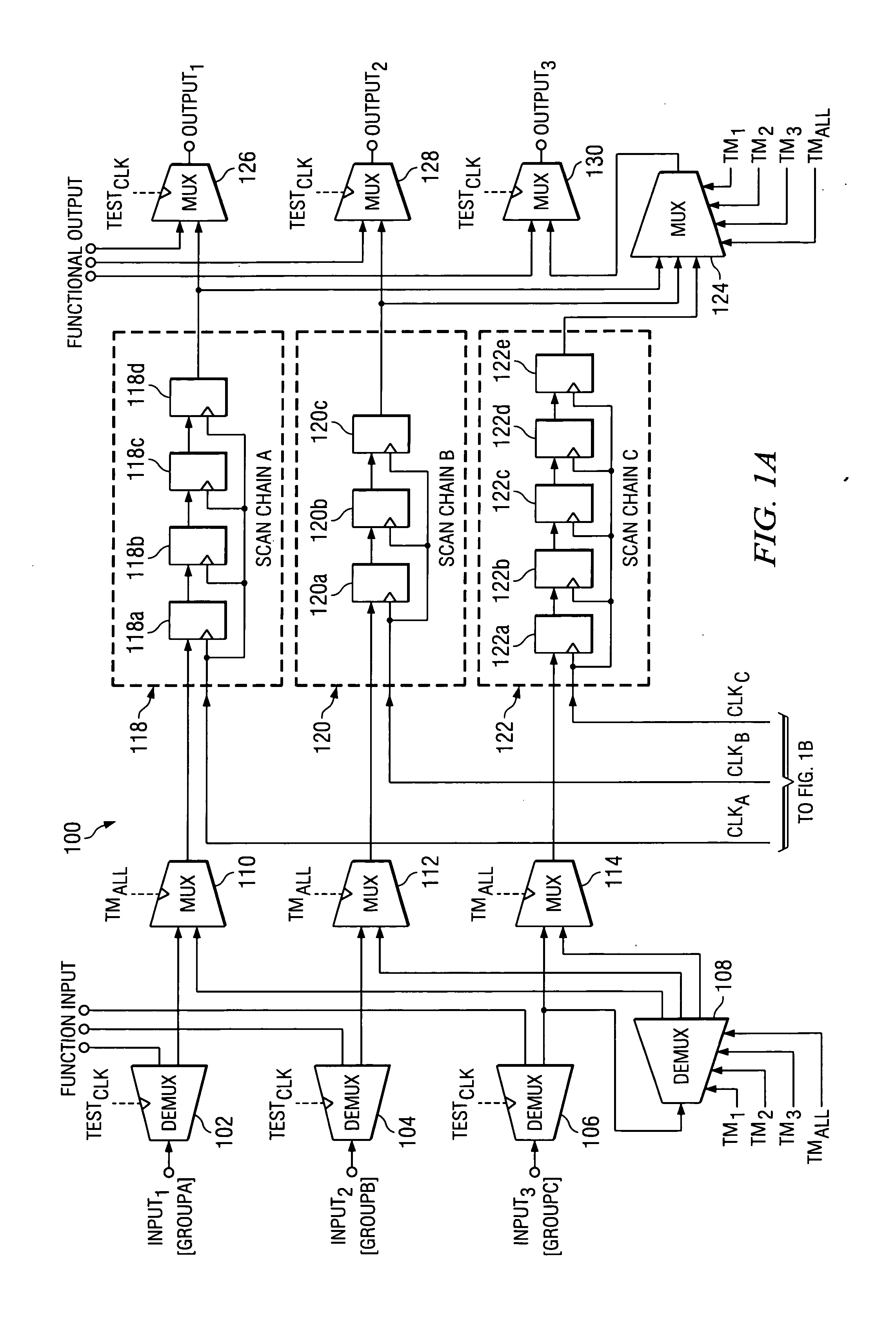
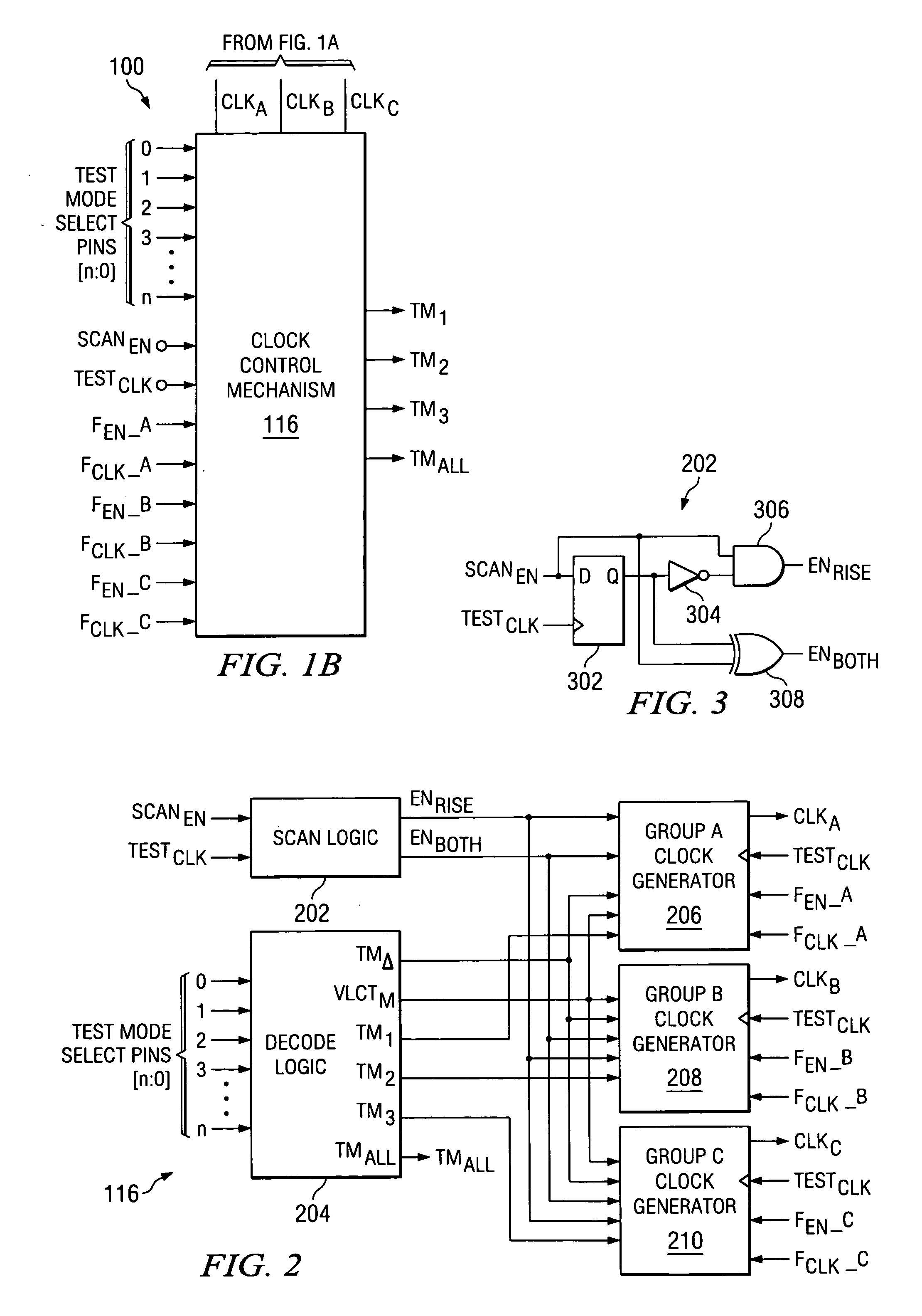
[0029] The present invention has been implemented on a Texas Instruments™ mixed signal SoC, Sangam™ (TNETD7300), which is a SoC that includes a MIPS processor and an asynchronous digital subscriber line (ADSL) physical layer (PHY) subsystem together with peripherals designed to serve as a single chip ADSL bridge or router device for residential and small office applications. Given the at-speed scan design in accordance with the present invention and its implementation on an ADSL CPE modem having analog and di...


PUM


Abstract

A scan test circuitry design imbedded on an SoC having the scan architecture of a VLCT platform is disclosed herein. This BIST circuitry design that is not limited in the number of scan test ports supported includes at least one scan chain group having a corresponding clock domain that couples to receive test stimulus data. Each scan chain group has a corresponding test mode signal to shift the test stimulus data at a shift clock rate derived from its corresponding clock domain. A controlling demultiplexer connects to each multiplexer unit within each scan chain group to provide control signals for shifting in the test stimulus. A clock control mechanism provides a control signal for each scan chain to shift test stimulus and capture resultant data. Furthermore, when a simultaneous test mode signal is enabled, the clock control mechanism couples to each scan chain to enable simultaneous capture of each scan chain group.

Description

FIELD OF THE INVENTION [0001] The present invention relates to an at-speed Automatic Test Pattern Generator (ATPG) for testing a System on Chip (SoC), and, more particularly, to at-speed testing for SoC Designs having multiple clock domains and frequencies that implement testing using the Very Low Cost Test (VLCT) platform. BACKGROUND OF THE INVENTION [0002] An Automatic Test Pattern Generator (ATPG) is a software design tool that simulates the overall functionality of the design or individual circuits within the design of an integrated circuit and generates test vectors for testing the overall functionality of the design. Through the use of these at-speed test vectors, an Automatic Testing Equipment (ATE) may provide a particular degree of fault coverage or fault simulation for the circuitry in the product. Specifically, automatic test pattern generation (ATPG) techniques may provide test patterns for stuck-at faults, transition faults and path delay faults. Conventionally, these t...

Claims


Application Information

Patent Timeline
IPC IPC(8): G01R31/3185
CPCG01R31/318552
Inventor AGASHE, ANUPAMA ANLRUDDHAKRISHNAMOORTHY, NIKILASAHA, ANLNDYAPAREKHJI, RUBIN A.
Owner TEXAS INSTR INC
Why Eureka
Try Eureka