Electrode, method for forming an electrode, thin-film transistor, electronic circuit, organic electroluminescent element, display, and electronic equipment

a thin-film transistor and electrode technology, applied in the direction of thermionic cathodes, discharge tubes/lamp details, discharge tubes luminescnet screens, etc., can solve the problems of low efficiency in injecting carriers (holes), lowering transistor properties, and reducing the efficiency of transistors, so as to enhance the property (switching property) of the thin-film transistor. , the effect of high reliability

Active Publication Date: 2005-03-17
E INK CORPORATION
View PDF6 Cites 76 Cited by
  • Summary
  • Abstract
  • Description
  • Claims
  • Application Information

AI Technical Summary

Benefits of technology

[0007] An exemplary aspect of the present invention provides an electrode that is economically produced and capable of efficiently injecting holes, a method to form an electrode that is capable of easily manufacturing such an electrode, a highly reliable thin-film transistor, an electronic circuit using this thin-film transistor, a highly reliable organic electroluminescent element, a display, and electronic equipment.
[0008] An electrode of one exemplary aspect of the present invention includes an oxide having at least one of Cu, Ni, Co on a surface of the electrode, at least on a side of an organic layer. The organic layer is mainly made of an organic material and has a function of transporting a hole. The electrode injects a hole into the organic layer. It is also possible to include an oxide not only in the surface but also all over the electrode. This enables the electrode to be economically manufactured and to efficiently inject a hole.
[0009] In an electrode of another exemplary aspect of the present invention, a content of the oxide may be 50 wt % or more in a portion where the oxide is included. This enhances efficiency in injecting a hole. In an electrode of another aspect of the present invention, the oxide may include at least one of Sr, Al, Ga, Li, Na, K, Rb, Cs in addition to Cu, Ni, Co. This increases electric conductivity and efficiency in injecting a hole.

Problems solved by technology

Vol. 98. No. 948354840, however, leaves room for improvement in terms of cost, since the source and drain electrodes are formed by depositing and etching a costly gold thin film.
If an alternative economical metal, such as aluminum, is used to form the electrodes, there arises a problem of lowering transistor properties as a result of a large barrier at the interface of the source electrode and the organic semiconductor layer, which results in low efficiency in injecting carriers (holes).

Method used


Image

  • Electrode, method for forming an electrode, thin-film transistor, electronic circuit, organic electroluminescent element, display, and electronic equipment
  • Electrode, method for forming an electrode, thin-film transistor, electronic circuit, organic electroluminescent element, display, and electronic equipment
  • Electrode, method for forming an electrode, thin-film transistor, electronic circuit, organic electroluminescent element, display, and electronic equipment

Examples


examples

[0189] Specific examples of exemplary aspects of the present invention will now be described.

[0190] A1. Manufacturing a Thin-Film Transistor

example a1

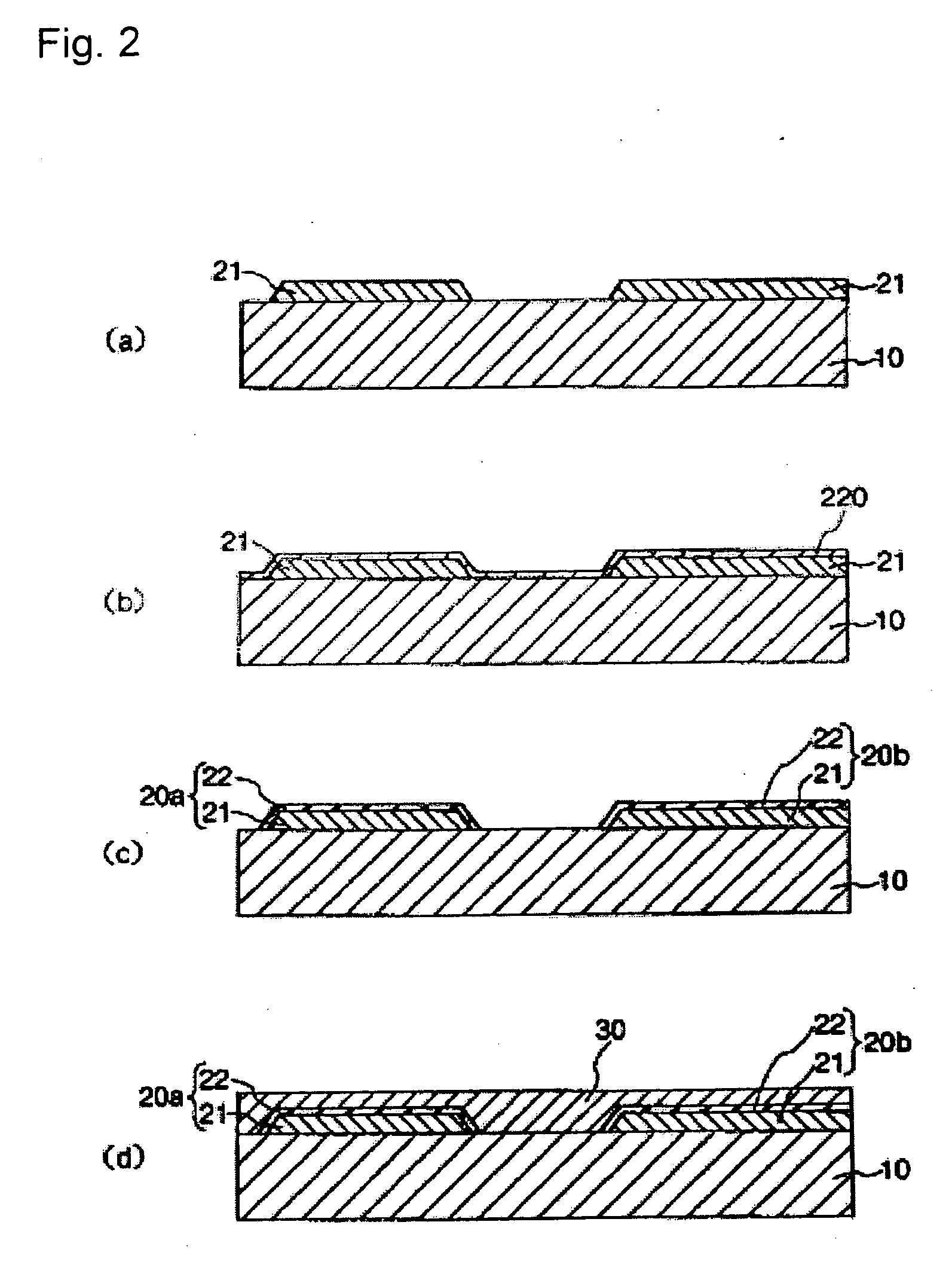
[0191] First, a glass substrate (OA10, made of NEC, Corning) was prepared and cleaned with ethanol so as to degrease its surface.

[0192] After being dried, the glass substrate was immersed in concentrated sulfuric acid so as to have a rough surface. This way, a plating film to be formed in the following step can have increased adhesiveness. Then, the glass substrate was washed with pure water. Next, a cycle of immersing the glass substrate in a sensitivity increasing liquid for 15 seconds and the washing the substrate with pure water was repeated four times. As the sensitivity increasing liquid, a solution (tin chloride (II) solution) of 37 wt % concentrated hydrochloric acid (1 mL / L) and SnCl2 (1 g / L) was used.

[0193] Subsequently, the glass substrate was immersed in a Ni plating bath for five minutes. The conditions of the Ni plating bath are as follows:

[0194] Sodium hypophosphite solution: 0.15 mol / L

[0195] Ammonium sulfate solution: 0.50 mol / L

[0196] Sodium acid citrate solutio...

example a2

[0209] A glass substrate was immersed in a 0.1 wt % nickel chloride solution to which dimethylborane as a reducer had been added at 40 degrees centigrade for five minutes, so as to form a Ni plating film. With the other steps being similar to the example A1, a thin-film transistor was completed. The average thickness of the Ni plating film was 100 nm.


PUM


Abstract

An electrode is provided that is economically produced and capable of efficiently injecting holes. Also provided are a method to form an electrode that is capable of easily manufacturing such an electrode, a highly reliable thin-film transistor, an electronic circuit using this thin-film transistor, an organic electroluminescent element, a display, and electronic equipment. A thin-film transistor is a top-gate thin-film transistor. The thin-film transistor includes a source electrode and a drain electrode that are placed separately from each other. The thin-film transistor also includes an organic semiconductor layer that is laid out between the source electrode and the drain electrode, and a gate insulating layer that is provided between the organic semiconductor layer and a gate electrode. This structure is mounted on a substrate. Each of the source electrode and the drain electrode is composed of two layers, that is, an underlying electrode layer and a surface electrode layer. The surface electrode layer includes an oxide containing at least one of Cu, Ni, Co, Ag.

Description

BACKGROUND OF THE INVENTION [0001] 1. Field of Invention [0002] The present invention relates to an electrode, a method to form an electrode, a thin-film transistor, an electronic circuit, an organic electroluminescent element, a display, and electronic equipment. [0003] 2. Description of Related Art [0004] Related art organic thin-film field-effect transistors using organic semiconductor materials may be potential substitutions for thin-film field-effect transistors using inorganic materials represented by silicon. Typical related art organic thin-film transistors have a structure using gold for their source and drain electrodes, as described in Rogers et al. 24 Apr. 2001. Proceedings of the National Academy of Sciences. Vol. 98. No. 948354840, for example. [0005] Specifically, a thin-film transistor described in Rogers et al. 24 Apr. 2001. Proceedings of the National Academy of Sciences. Vol. 98. No. 948354840 has a structure in which a gate electrode is formed by etching indium t...

Claims


Application Information

Patent Timeline
Patent Type & Authority Applications(United States)
IPC IPC(8): H01L21/02H01L21/28H01L51/50H01L29/417H01L29/43H01L29/786H01L51/00H01L51/05H01L51/10H01L51/40H05B33/00H05B33/10H05B33/26
CPCH01L51/0021H01L51/105H01L51/0545H01L51/0541H10K71/60H10K10/466H10K10/464H10K10/84H05B33/26H05B33/00H05B33/10
Inventor MORIYA, SOICHIKAWASE, TAKEOHARADA, MITSUAKI
Owner E INK CORPORATION
Why Eureka
Try Eureka