Field emission device

ield emission technology, applied in the field of field emission devices, can solve the problems of leakage current, difficult formation of self-aligning electron emitting gates, and difficulty in implementing a large area display of such a field emission device, and achieve the effect of facilitating control of electron emission and reducing leakage curren

Active Publication Date: 2005-03-17
ELECTRONICS & TELECOMM RES INST
View PDF8 Cites 30 Cited by
  • Summary
  • Abstract
  • Description
  • Claims
  • Application Information

AI Technical Summary

Benefits of technology

[0018] The present invention is also directed to a field emission device, which reduces a leakage current flowing into the gate as an electron emitting electrode and facilitates control of electron emission.
[0019] The present invention is also directed to a field emission device, which allows most electrons to be emitted in the carbon nanotube or carbon nanofiber arranged near the gate electrode to thereby overcome the potential leakage current and spreading of the electron beam.

Problems solved by technology

Thus, while a fine pattern should be formed and a self-alignment scheme by means of electron beam evaporation should be performed in the above-mentioned procedure, there is difficulty in application of such a field emission device for implementing a large area display.
However, when they are used as the electron emission source by means of an electric field, it is not easy to form a self-aligned electron emitting gate so as to have a structure capable of readily inducing and controlling electron emissions compared to the Spindt-type metal tip of FIG. 1.
Thus, the emitted electrons flow into the gate to result in a leakage current.
In addition, the gate opening is larger compared to the thickness of the insulator, which causes difficulty in controlling electron emission due to an anode voltage, and causes the emitted electron beam to be widely spread when it reaches the anode as compared to its emitting instance.
These phenomena deteriorate the properties of the field emission device, and in particular, they may cause a significant problem when the field emission device is applied for a flat panel display.

Method used


Image

  • Field emission device
  • Field emission device
  • Field emission device

Examples


first embodiment

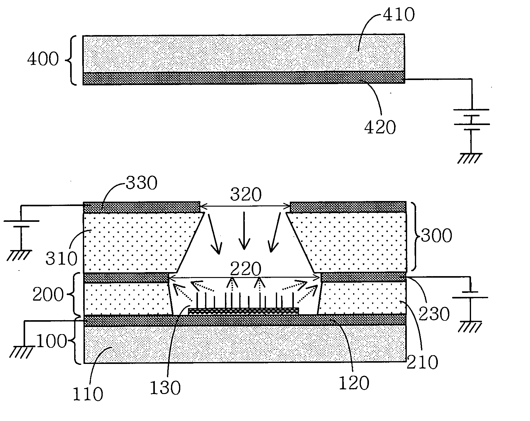
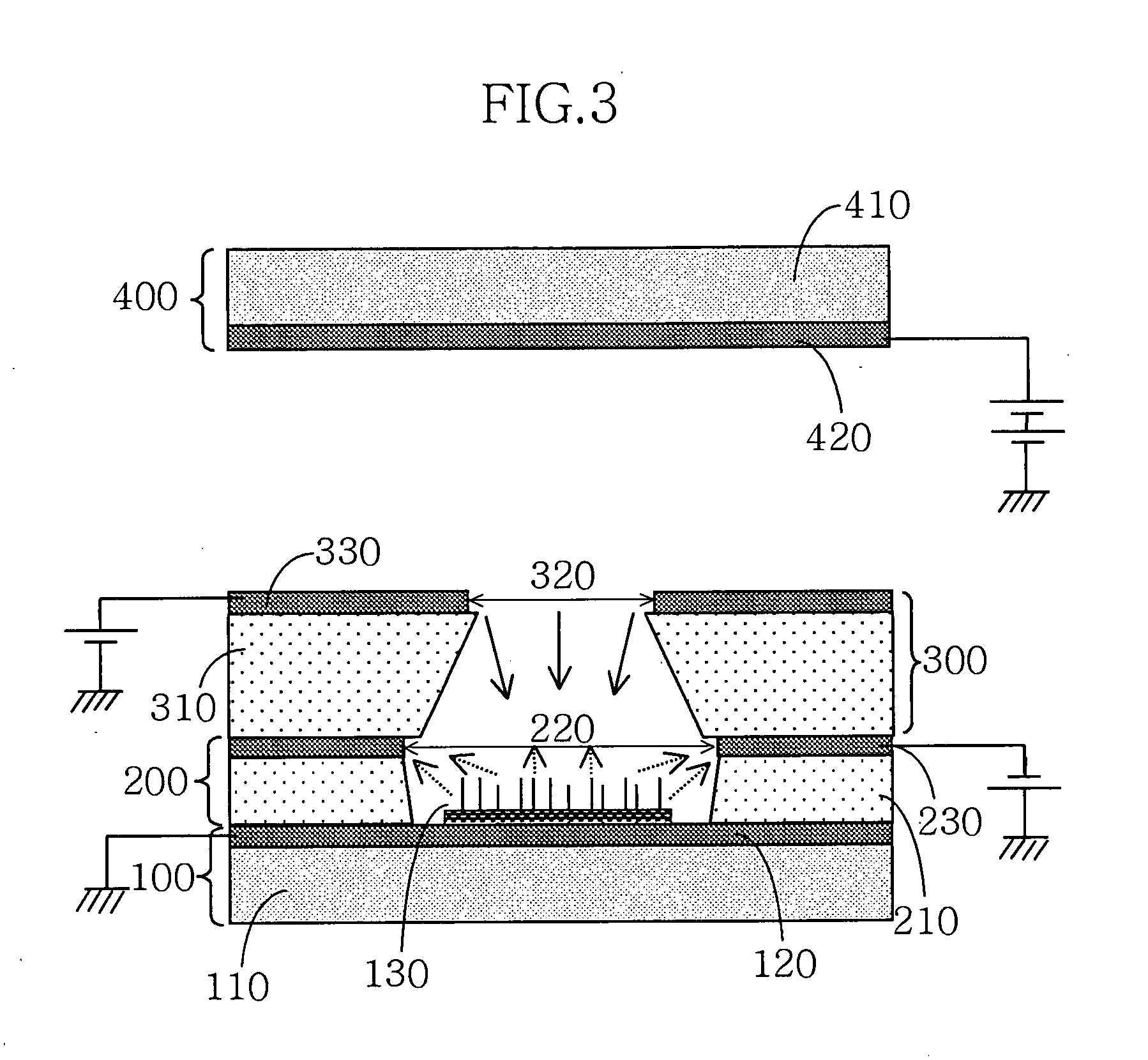
[0031]FIG. 3 is a diagram illustrating a schematic configuration of a field emission device in accordance with a first embodiment of the present invention.

[0032] The field emission device of FIG. 3 comprises a cathode 100, a field emission suppressing gate 200, a field emission inducing gate 300, and an anode 400. This field emission device corresponds to one dot pixel in the field emission display, and a plurality of dot pixels are arranged in a matrix form and a plurality of interconnection lines are also included to apply various signals to each of the dot pixels in an actual process for fabricating the field emission display.

[0033] Each of the cathode 100, field emission suppressing gate 200, field emission inducing gate 300, and anode 400 may be formed on a separate substrate, or the cathode 100 and field emission suppressing gate 200 may be formed on one substrate, and the field emission inducing gate 300 and anode 400 may be formed on another substrate. Alternatively, the c...

second embodiment

[0056] Next, the field emission device in accordance with a second embodiment of the present invention will be described in detail with reference to FIG. 6 to FIG. 8. For simplicity of description, the difference between the first and second embodiments will be described in detail. FIG. 6 is a diagram illustrating a schematic configuration of a field emission device in accordance with the second embodiment of the present invention. FIG. 7 is a cross sectional view for explaining a configuration of one dot pixel in a field emission display in accordance with the second embodiment of the present invention. FIG. 8 is a plan view of a pixel array for explaining the structure in which the pixels of FIG. 7 are arranged in a matrix form.

[0057] The second embodiment differs from the first embodiment in that the field emission suppressing gate opening is separated into at least two regions. Each region has a separate electric field emitter.

[0058] In accordance with the second embodiment, i...


PUM


Abstract

A field emission device including a cathode having an electric field emitter for emitting electrons, a field emission inducing gate for inducing electron emission, and an anode for receiving the emitted electrons. A field emission suppressing gate is interposed between the cathode and the field emission inducing gate for suppressing electron emission, so that problems such as gate leakage current, electron emission due to anode voltage, and electron beam spreading of the conventional field emission device are significantly overcome.

Description

BACKGROUND [0001] 1. Field of the Invention [0002] The present invention relates to a field emission device, and more particularly, to a field emission device comprising a field emission suppressing gate for suppressing electron emission which is interposed between a cathode and a field emission inducing gate. [0003] 2. Discussion of Related Art [0004] Field emission devices have been widely used as an electron source of a microwave element, a sensor, a flat panel display, or the like, which emits electrons from a cathode electrode when an electric field is applied to the same in a vacuum or a specific gas atmosphere. [0005] Efficiency of electron emission significantly depends on an element structure, an emitter material, and an emitter shape in the field emission device. At present, the structure of the field emission device is mainly classified into a diode type consisting of a cathode and an anode, and a triode type consisting of a cathode, a gate, and an anode. [0006] The catho...

Claims


Application Information

Patent Timeline
Patent Type & Authority Applications(United States)
IPC IPC(8): H01J1/30H01J29/04H01J1/304H01J3/02H01J31/12
CPCH01J3/022C01B32/05H01J1/30
Inventor SONG, YOON HOHWANG, CHI SUNKIM, KWANG BOK
Owner ELECTRONICS & TELECOMM RES INST
Why Eureka
Try Eureka