Method of measuring meso-scale structures on wafers

Inactive Publication Date: 2005-03-17
TOKYO ELECTRON LTD
View PDF13 Cites 27 Cited by
  • Summary
  • Abstract
  • Description
  • Claims
  • Application Information

AI Technical Summary

Benefits of technology

It is another object of the present invention to provide a fast and robust means for characterizing dishing, erosion and residue of structures employed in microelectronic devices, e.g., integrated circuits. Depending on the situation in the factory, the hardware to make such measurements could be integrated into a process tool, such as a tool for chemical mechanical polishing (CMP), or on its own platform as a stand-alone tool.
It is another object of the present invention to provide a way to control the fabrication of microelectronic devices to minimize the occurance of dishing and erosion, on the one hand, and residue, on the other. Control of the process involves measuring the results of a process step and either feeding those results back to adjust the process for subsequent samples, or feeding the information forward to adjust subsequent processing steps.
Accord

Problems solved by technology

The presence of residue 150 is problematic because it is not part of the planned semiconductor structure and thus will, in all likelihood, interfere with the performance of the resulting device.
Unfortunately, the most effective method presently available for determining if residue is present on a wafer appears to be visual inspection of the wafer surface after it has been polished.
This is a time-consuming and labor-intensive process.
This is a serious limitation since the process in question may leave residue over structures that are laterally heterogeneous over the spot size of the instrument.
Since these features are smaller than the wavelength of light, it is not possible to focus between the features, making this method unsuitable for measuring such residue.
The presence of dishing and erosion are problematic for a number of reasons.
Metal loss raises the resistance of such lines, where resistance is typically critical because the lines are narrow.
The higher resistance can degrade device performance.
Dishing and erosion also cause an undesirable lack of planarity.
Lack of planarity on the current polished surface frequently leads to lack of planarity of the next, higher polished surface, especially when the processes that deposit the overlying layers are conformal

Method used


Image

  • Method of measuring meso-scale structures on wafers
  • Method of measuring meso-scale structures on wafers
  • Method of measuring meso-scale structures on wafers

Examples


second embodiment

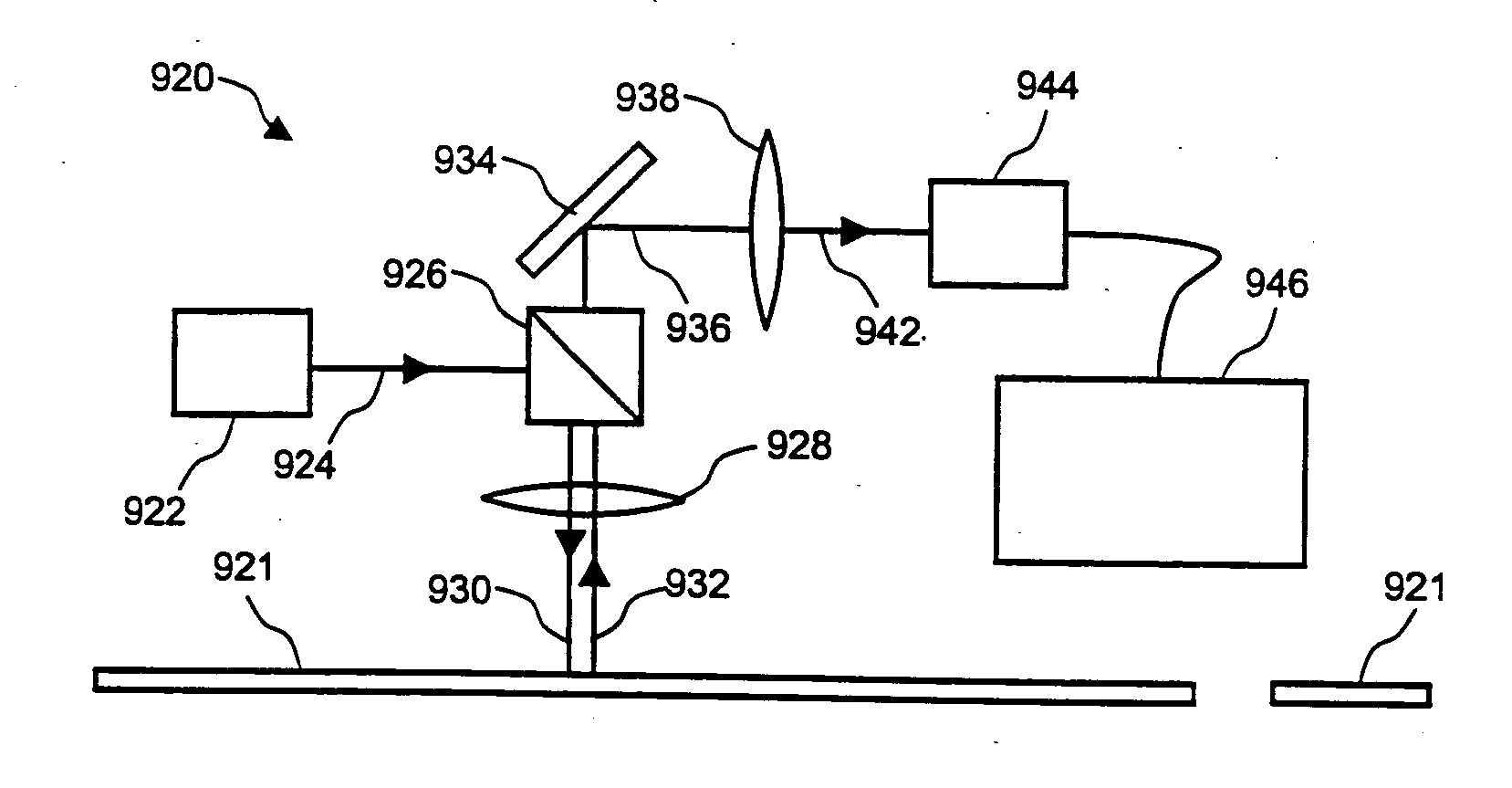
With reference to FIG. 13 and flow diagram 520, in the invention, the flow diagram 500 of FIG. 10 is embedded in flow diagram 520 routine 520 to measure at least one of the parameters in the model of step 500.

In step 522 of flow diagram 520, all the parameters needed to calculate the total reflectance are identified as either known or unknown. Parameters include the optical indices of all media that are illuminated, all significant geometric parameters, and the mixing parameters discussed above. The optical indices may be expressed as either functions of one or more parameters, as a table of values, or by some combination of the two methods. The precise form of the mixing parameters is chosen. Also the wavelengths to be considered are chosen.

In step 524, the values for all the known parameters are determined. These may be determined by measurements, experience, theoretical considerations, or any other means.

In step 526, estimated values are assigned to all the unknown parameter...

third embodiment

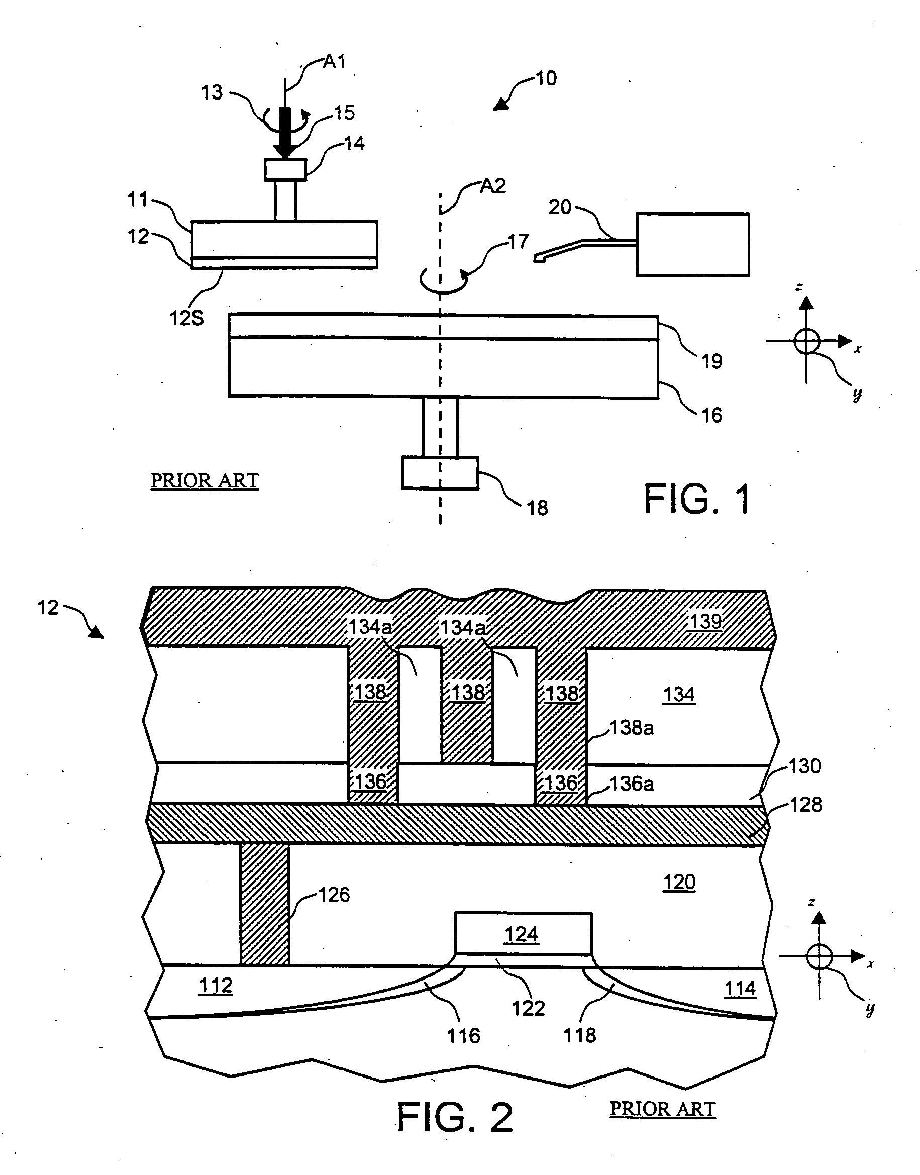
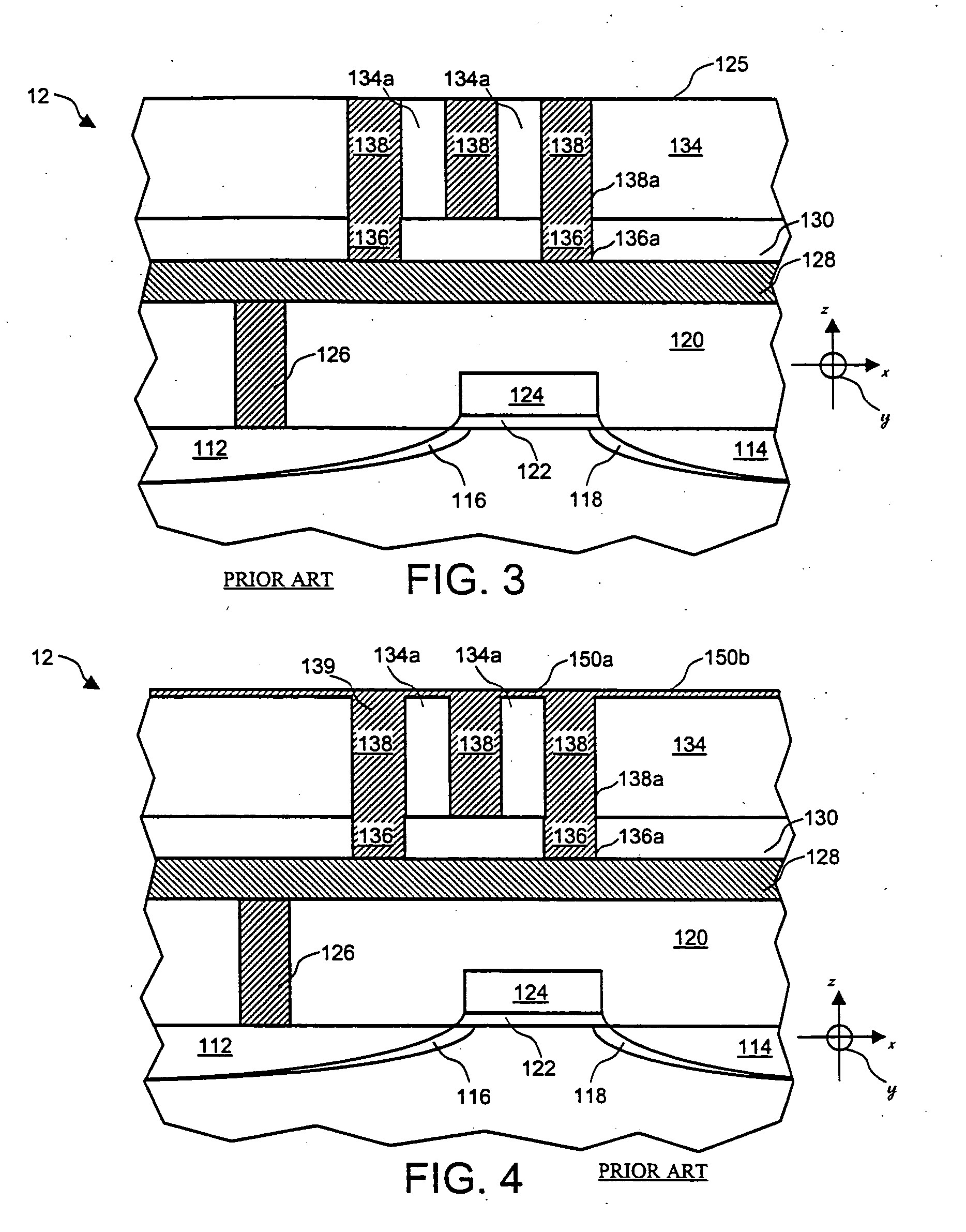
With reference to FIGS. 15a, 15b and 16, an example of the present invention that uses a collection of sites and a chain of algorithms to measure unknown wafer parameters of interest is now described. FIG. 16 shows the flow diagram for a more general procedure. With reference to FIGS. 15a and 15b, die 650 on the wafer contains two sites of interest, 652 and 654. These sites are regarded as a collection of sites, i.e., they are measured sequentially over spots 653 and 655, respectively, and then processed together by a chain of algorithms. As the term is used herein, a chain or collection of algorithms comprises a set of algorithms that are linked by passing parameters of one algorithm to another algorithm in the chain or collection. The parameter may become either a fixed value in the destination algorithm, or an initial estimate for that algorithm. Site 652 comprises a stack of uniform films, and site 654 is an array, as described above. In general, site 652 is easier to measure an...


PUM

PropertyMeasurementUnit
Structureaaaaaaaaaa
Reflectionaaaaaaaaaa
Reflectanceaaaaaaaaaa

Abstract

A method of measuring at least one parameter associated with a portion of a sample having formed thereon one or more structures with at least two zones each having an associated zone reflectance property. The method includes the steps of illuminating the zones with broadband light, and measuring at least one reflectance property of light reflected from the at least two zones. The measurement includes a substantial portion of non-specularly scattered light, thereby increasing the quality of the measurement. The method further includes the step of fitting a parameterized model to the measured reflectance property. The parameterized model mixes the zone reflectance properties of the zones to account for partially coherent light interactions between the two zones.

Description

FIELD OF THE INVENTION The present invention pertains to processing wafers, and in particular to measuring parameters indicative of the quality of the wafer processing. BACKGROUND OF THE INVENTION Chemical-mechanical polishing (CMP) is a well-known process in the semiconductor industry used to remove and planarize layers of material deposited on a semiconductor device to achieve a planar topography on the surface of the semiconductor device. To remove and planarize the layers of the deposited material, including dielectric and metal materials, CMP typically involves wetting a pad with a chemical slurry containing abrasive components and mechanically polishing the front surface of the semiconductor device against the wetted pad to remove the layers of deposited materials on the front surface of the semiconductor device and planarize the surface. FIG. 1 is a schematic view of a prior art CMP apparatus 10. CMP apparatus 10 includes a wafer carrier 11 for holding a semiconductor wafer...

Claims


Application Information

Patent Timeline
IPC IPC(8): G01B11/06G01B11/30G01N21/21G01N21/95H01L21/66H01L21/67
CPCG01B11/0625G01B11/30H01L22/12G01N21/9501H01L21/67G01N21/211
Inventor JOHNSON, KENNETH C.STANKE, FRED E.
Owner TOKYO ELECTRON LTD
Why Eureka
Try Eureka