

Memory devices based on electric field programmable films
a technology of programmable films and memory devices, applied in solid-state devices, nanoinformatics, instruments, etc., can solve the problems of high power consumption, complex structure, high fabrication cost, etc., and achieve the effect of reducing production costs, simple structure, and high device density
- Summary
- Abstract
- Description
- Claims
- Application Information
AI Technical Summary
Benefits of technology
Problems solved by technology
Method used
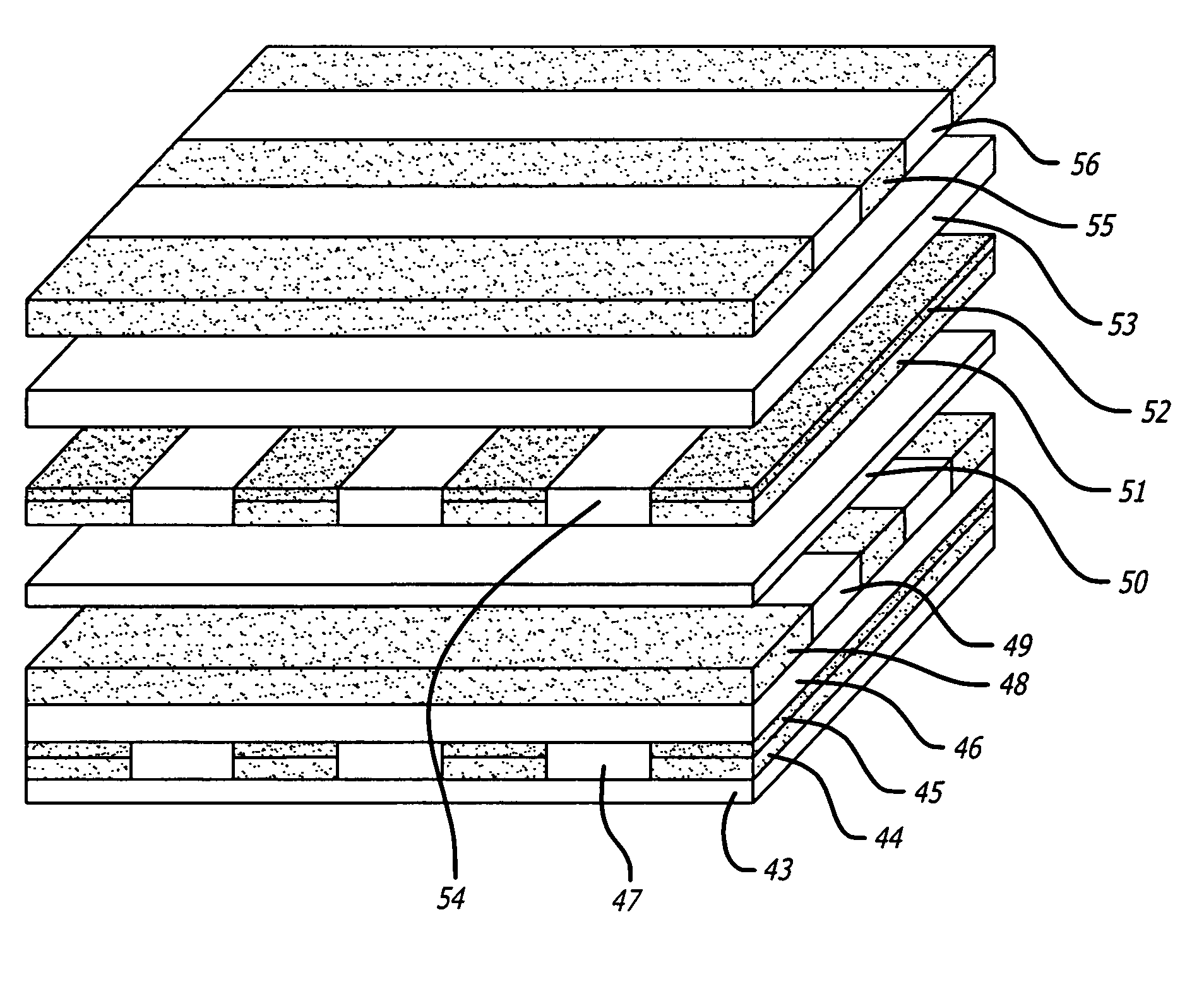
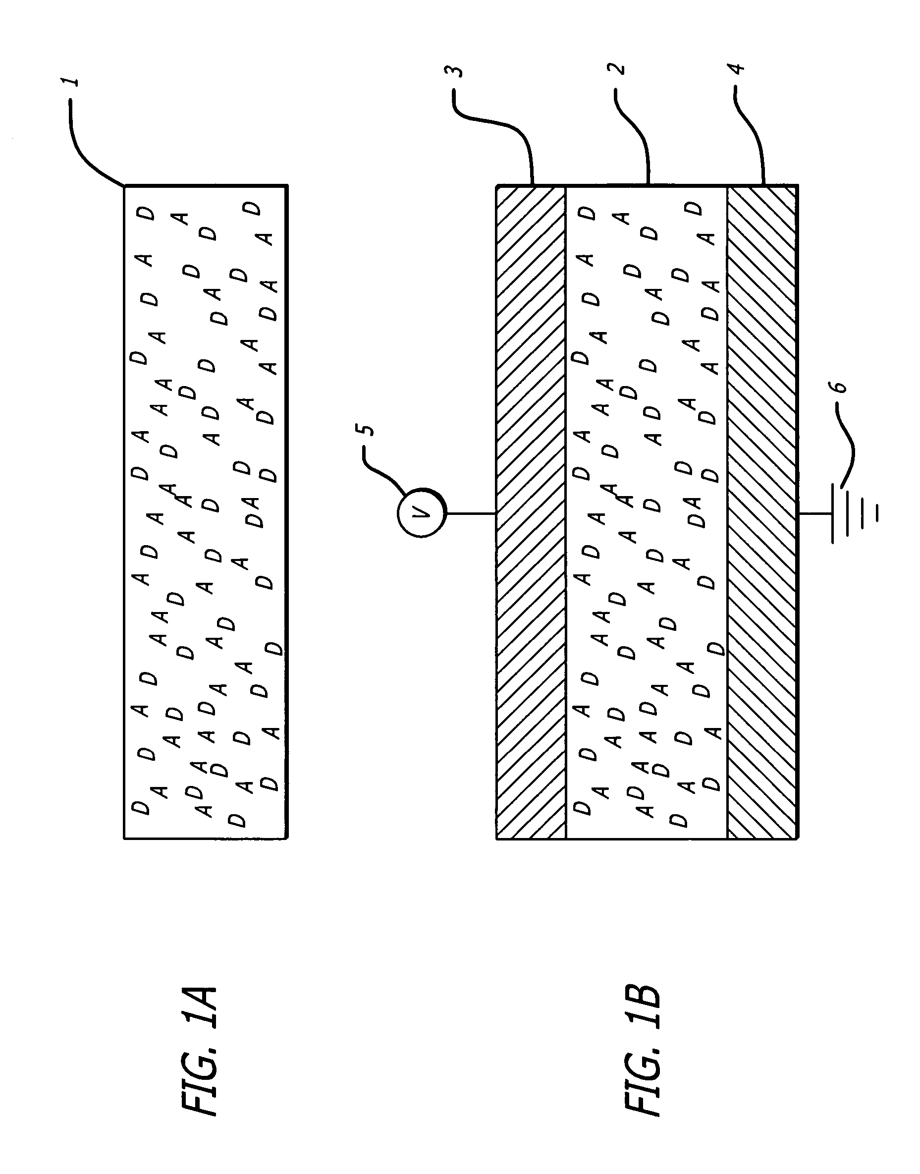
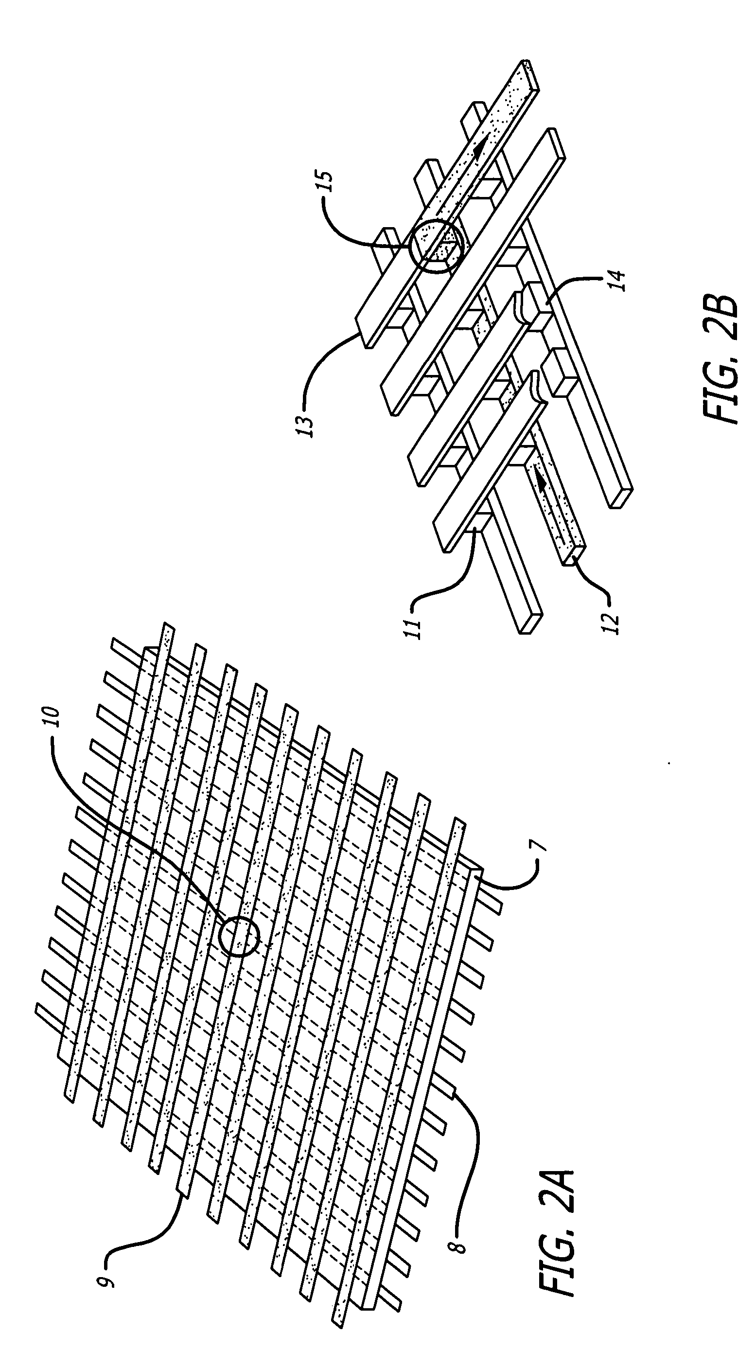
Image

Examples
example 1
Gold nanoparticles were synthesized at room temperature using a two-phase arrested growth method detailed by M. J. Hostetler, et. al., Langmuir, 14 (1998) 17). 50 milliliter (ml) aqueous solution of 0.62 grams (g) HAuCl4.3H2O (2 equiv) was added into 80 ml toluene solution of 3.0 g of tetraoctylammonium bromide (5 equiv). The mixture was vigorously stirred for 1 hour. The organic phase was collected and 0.4 ml dodecanethiol was added to the reaction mixture. The resulting solution was stirred for 10 minutes (min) at room temperature. The solution was then stirred vigorously and 50 ml aqueous solution of NaBH4 (0.76 g, 20 equiv) was added over a period of 15 min. The mixture was further stirred at room temperature for 1 hour (h). The organic phase was then collected, and the gold nanoparticles were precipitated by adding 400 ml methanol. The black precipitate was separated from the solution. 20 ml tetrahydrofuran was used to dissolve the black precipitate and another 200 ml methanol...
example 2
Gold nanoparticles were prepared by the same process as Example 1 except that 0.6 ml dodecanethiol was added during the chemical reaction.
example 3
Gold nanoparticles were prepared by the same process as Example 1 except that 0.8 ml dodecanethiol was added during the chemical reaction.
PUM
| Property | Measurement | Unit |
|---|---|---|
| Dielectric constant | aaaaa | aaaaa |
| Electric field | aaaaa | aaaaa |
Abstract
Description
Claims
Application Information