

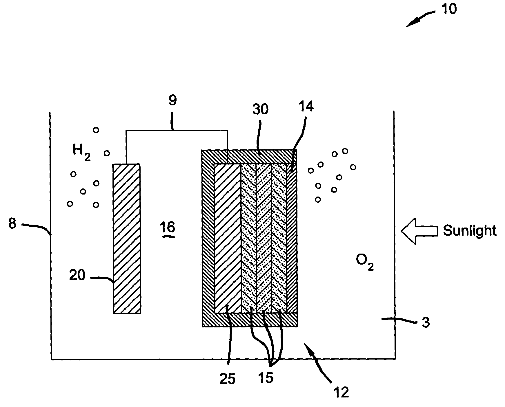
Photoelectrochemical device and method of making
- Summary
- Abstract
- Description
- Claims
- Application Information
AI Technical Summary
Benefits of technology
Problems solved by technology
Method used
Image


Examples
example
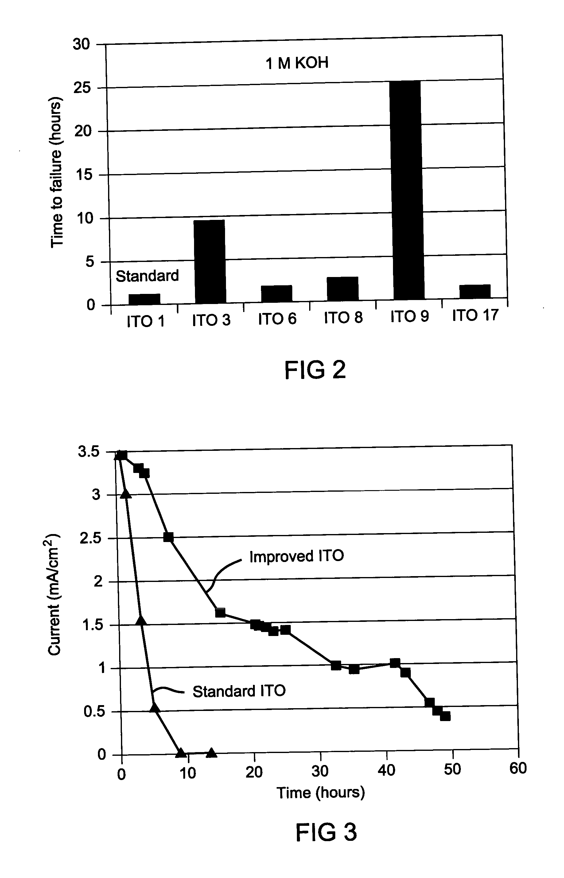
[0033] The samples were prepared using a process called “sputtering”. In this process a target of 90% indium oxide, In2O3 and 10% tin oxide SnO2 was bombarded by argon ions, Ar+, from a sputter gun in a vacuum chamber. The Ar+ ions dislodge (sputter) material from the target and in a high vacuum chamber the material (ITO) was focused with a magnetron and condensed onto the receiving substrate which was a 2″×2″ stainless steel plate covered by a shadow mask as described below. A total of 20 samples of ITO on stainless steel were prepared and the six listed in Table I were tested using suitable electrochemistry apparatus, to determine the surface coating (ITO) corrosion rates.
[0034] Sputtering conditions for six samples tested are shown in Table 1 below which explores some of the sputtering conditions. Basic sputter apparatus and basic operation of same is as described in X. Deng, G. Miller, R. Wang, L. Xu and A. D. Compaan, “Study of sputter deposition of ITO films for a-Si:H n-1-p ...
PUM
| Property | Measurement | Unit |
|---|---|---|
| thickness | aaaaa | aaaaa |
| thickness | aaaaa | aaaaa |
| temperature | aaaaa | aaaaa |
Abstract
Description
Claims
Application Information