Near-field light source device, and optical head, optical device, exposure apparatus and microscope device having such near-field light source device

a near-field light source and light source technology, which is applied in the direction of optical beam sources, instruments, semiconductor lasers, etc., can solve the problems of insufficient light intensity stability, simple reinforcing of light as disclosed in u.s. patent no. 6,236,033 mentioned above, etc., and achieve low threshold value, stable oscillation mode, good efficiency

Inactive Publication Date: 2005-03-24
CANON KK
View PDF9 Cites 17 Cited by
  • Summary
  • Abstract
  • Description
  • Claims
  • Application Information

AI Technical Summary

Benefits of technology

It is accordingly an object of the present invention to provide a near-field light source device of low threshold value, good efficiency and stable oscillation mode, whereby near-field light of less variation of light intensity and having an increased intensity can be produced.

Problems solved by technology

However, in order to meet strict requirements of recent next-generation high-density recording technology or super-fine exposure technology, as described above, the near-field light source based on a ring resonator type semiconductor laser as disclosed in Japanese Laid-Open Patent Application, Publication No. 2001-326420 mentioned above is not fully satisfactory in respect to the stability of light intensity, for example.
Further, simply reinforcing the light as disclosed in U.S. Pat. No. 6,236,033 mentioned above is still insufficient.

Method used


Image

  • Near-field light source device, and optical head, optical device, exposure apparatus and microscope device having such near-field light source device
  • Near-field light source device, and optical head, optical device, exposure apparatus and microscope device having such near-field light source device
  • Near-field light source device, and optical head, optical device, exposure apparatus and microscope device having such near-field light source device

Examples


embodiment 1

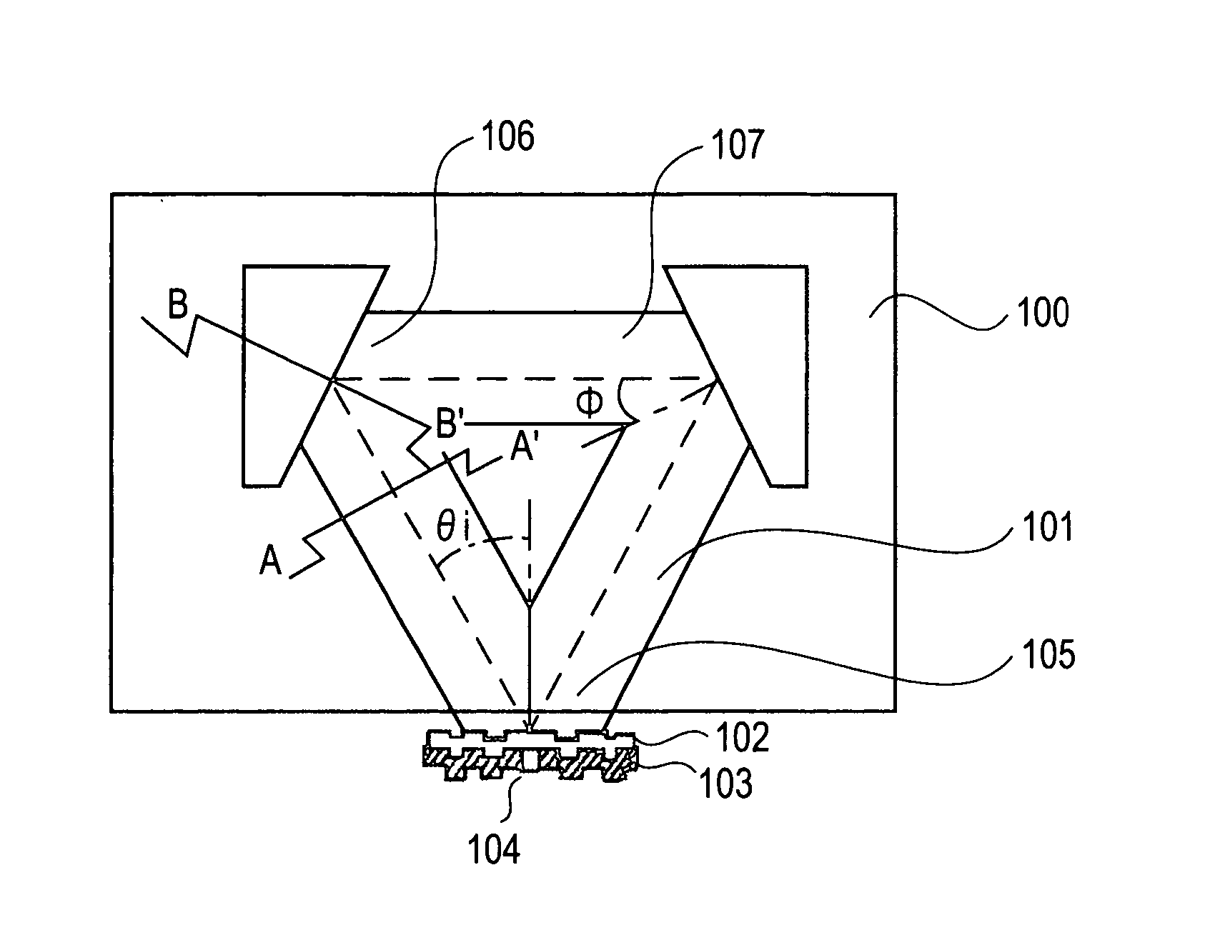
A first embodiment of the present invention will be described with reference to an example of near-field light source device shown in FIGS. 1A, 1B and 1C. Details of the structure of the near-field light source device 100 shown in FIGS. 1A-1C are as has been described hereinbefore.

In this embodiment, the near-field light source device 100 was manufactured in the following manner.

First, a semiconductor multilayer structure such as shown in the sectional view of FIG. 1C taken along a line A-A′ was formed in accordance with a vapor-phase epitaxy method. More specifically, n-AlGaAs clad layer 112, AlGaAs / AlGaAs quantum well activating layer 113, p-AlGaAs clad layer 114 and p-GaAs cap layer 115 were formed on an n-GaAs substrate 111 in accordance with crystal growth. A photoresist was applied and, through mask pattern exposure and development, a resist pattern of ring resonator shape was formed. By means of reactive ion etching using a chlorine gas, a part of the p-clad layer 114 wa...

embodiment 2

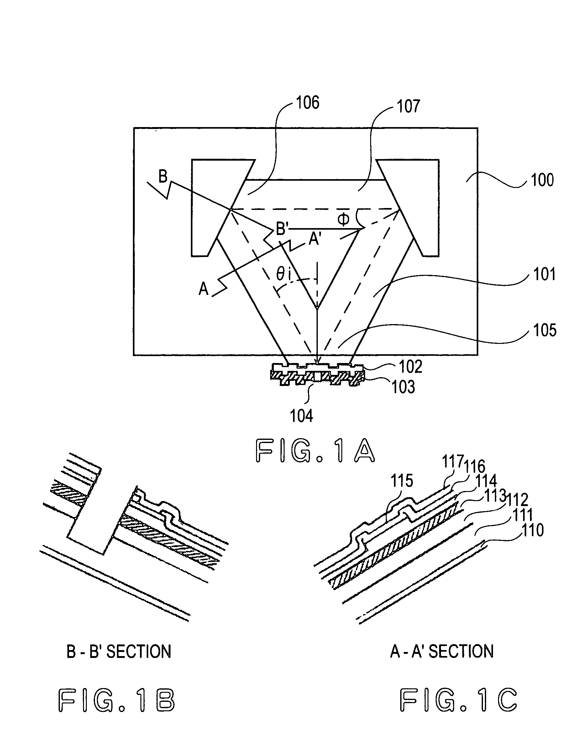
FIG. 2 shows the structure of a near-field light source device according to a second embodiment of the present invention. In this embodiment, each of the clockwise rotation mode and the counterclockwise rotation mode is accomplished by negative first order light from a diffraction grating.

In FIG. 2, denoted at 200 is a near-field light source device of the present invention. A light blocking film on a mirror comprises a dielectric material film 201 and a metal film 202, and it is formed with periodic surface irregularity so that it can function as a diffraction grating. A small opening 203 is formed in this metal film. Denoted at 205 is a reflection surface to be described later in detail.

Denoted at 206 is a corner mirror having a diffraction grating, and denoted at 207 and 208 are plane corner mirrors that constitute a ring resonator.

The layer structure as a semiconductor laser and the method of producing the same are similar to those in the first embodiment.

The second embo...

embodiment 3

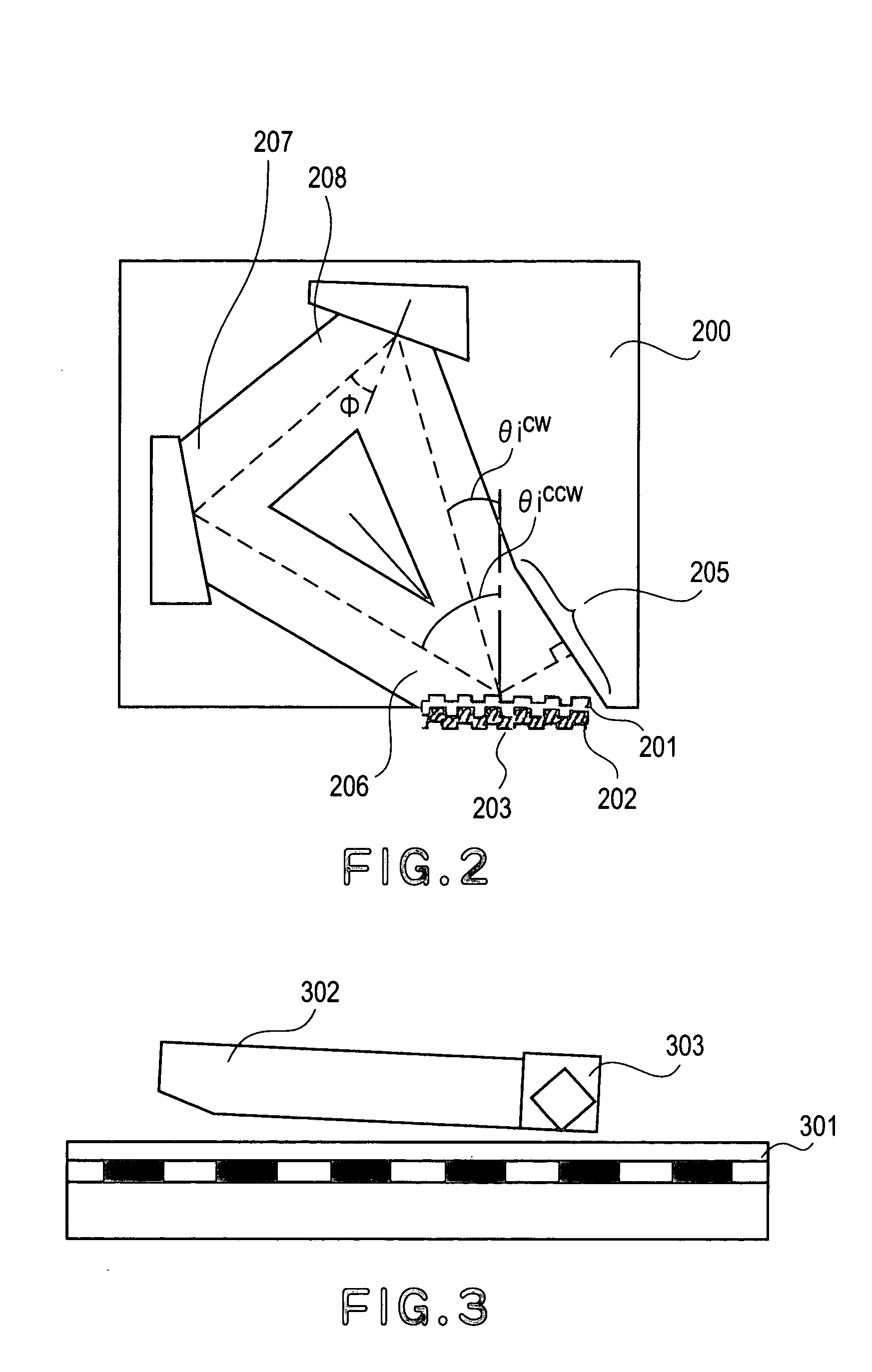
FIG. 4 shows the structure of an exposure apparatus according to a third embodiment of the present invention.

Denoted in FIG. 4 at 1001 is a near-field light source of the present invention, and denoted at 1002 is a cantilever. Denoted at 1003 is a wafer stage, and denoted at 1004 is a piezoelectric device. Denoted at 1005 is a position detecting semiconductor laser, and denoted at 1006 is a half-split sensor. Denoted at 1007 is a wafer, and denoted at 1008 is a resist film on the wafer. The resist thin film 1008 being sensitive to near-field light around a small opening of the near-field light source is applied to the wafer 1007 surface. The near-field light source 1001 is mounted on the cantilever 1002, and by means of the piezoelectric device 1004 the distance from the wafer stage 1003 or from the resist film 1008 of the wafer surface mounted on the wafer stage can be controlled. Specifically, this distance can be controlled in accordance with the principle of optical lever such...


PUM

PropertyMeasurementUnit
total reflection critical angleaaaaaaaaaa
wavelength sizeaaaaaaaaaa
electric field vectoraaaaaaaaaa

Abstract

Disclosed are a near-field light source device as well as an optical head, an optical device, an exposure apparatus and a microscope device having such near-field light source device. As an example, the near-field light source device has a semiconductor laser having a ring-type optical resonator with a plurality of wave guides connected via mirror portions, a light blocking film formed in one of the mirror portions and having a small opening not greater than a wavelength size, and a diffraction grating formed on the light blocking film, wherein light oscillated from the semiconductor laser is diffracted by the diffraction grating, and the diffracted light is coupled to a rotation mode in the ring-type optical resonator.

Description

FIELD OF THE INVENTION AND RELATED ART This invention relates to a near-field optical device. More particularly, the invention concerns a near-field light source device using a ring resonator type semiconductor laser, and an optical head, an optical device, an exposure apparatus and a microscope device having such near-field optical device. In recent years, developments are being furthered in the fields of high-resolution observation technology, next-generation high-density recording technology and super-fine exposure technology, for example, on the basis of optical technology using evanescent light that leaking from a small opening of an order of 100 nm or less formed at a free end of a sharp probe, i.e., using what is called a near-field optical system. As a near-field light source to be used in high-density recording such as described above, Japanese Laid-Open Patent Application, Publication No. 2001-326420 discloses a ring resonator type semiconductor laser having a ring-shap...

Claims


Application Information

Patent Timeline
Patent Type & Authority Applications(United States)
IPC IPC(8): G01Q60/18G11B7/135G11B7/12G11B7/125G11B7/127G11B7/1353G11B7/1387H01S3/083H01S5/042H01S5/10H01S5/12H01S5/14H01S5/22H01S5/223
CPCG11B7/127G11B7/1353G11B7/1387H01S5/0425H01S5/2231H01S5/1085H01S5/141H01S5/2214H01S5/1071H01S5/04254
Inventor MIZUTANI, NATSUHIKOYAMADA, TOMOHIRO
Owner CANON KK
Why Eureka
Try Eureka