Light emitting array with improved characteristics, optical writing unit, and image forming apparatus

a technology optical writing units, applied in the field of light emitting arrays, can solve the problems of preventing the formation of satisfactory picture images, increasing power consumption, and being difficult to achieve, and achieve the effect of improving the quality of picture images

Inactive Publication Date: 2005-03-31
RICOH KK
View PDF15 Cites 109 Cited by
  • Summary
  • Abstract
  • Description
  • Claims
  • Application Information

AI Technical Summary

Benefits of technology

Accordingly, it is an object of the present invention to provide a light emitting array, having most, if not all, of the advantages and features of similar employed units, while eliminating many of the aforementioned disadvantages.
Thus, it becomes feasible that electrophotographic images can be output with excellent image characteristics at higher speeds, and that images in a certain color on demand can be output at higher speeds.

Problems solved by technology

Since the light scanning system utilizes a light deflector for scanning light beams as described above, its optical path length is relatively large to thereby give rise to a drawback of this system.
The noted means for increasing current input, however, results in a concomitant increase of power consumption.
This is, however, considered difficult at present since a rod lens array is hard to be formed so as to attain light spot characteristics uniform enough over receptor area for obtaining satisfactory pictorial images while maintaining the opening ratio improvement, as well.
Thus, there gives rise to a drawback of this method in which the variation of the shape of microlenses manifests itself as that of the characteristics of light spots on the photoreceptor, and this may prevent the formation of satisfactory picture images.
Although it is thus necessary to form uniform microlenses to form excellent images, such images are difficult to be acquired under the present conditions.
In addition, it is also difficult the light beams emanated from light emitting diodes are all led to form spots on the photoreceptor (the proportion of 90 percent level is cited in the application '991).
As a result, there gives rise to a drawback in which the variation of the shape of microlenses reveals itself as that of the characteristics of light spots on the photoreceptor, and this may prevent the formation of satisfactory picture images.
In addition, a further drawback is alluded to in that process steps required for forming the light guide structure are complicated because the light guides are formed by etching and their lens portions have to be fabricated through photolithography and etching process steps.
In the method described in the application '605, however, difficulties may arise.
This may unduly affect the transmission efficiency.
In the method described above in the application '579, however, since the microlens is provided directly on a light emitting plane of the light emitting element, it is difficult to make the apex height for the microlens larger than its curvature radius, and accordingly to reduce the radiation angle of the light beams emanated from the light emitting element.
This may result in drawbacks such as difficulty in forming micro mirrors having proper thickness and / or unduly enlarged light spot caused by light reflected by mirror surfaces and the method does not appear favorable in practice.

Method used


Image

  • Light emitting array with improved characteristics, optical writing unit, and image forming apparatus
  • Light emitting array with improved characteristics, optical writing unit, and image forming apparatus
  • Light emitting array with improved characteristics, optical writing unit, and image forming apparatus

Examples


Embodiment Construction

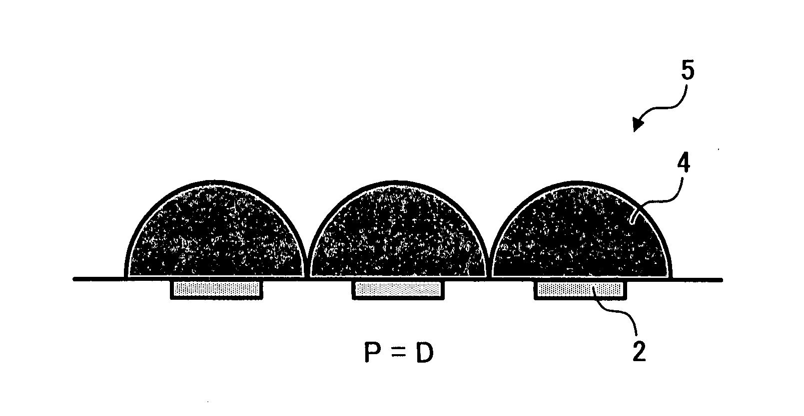
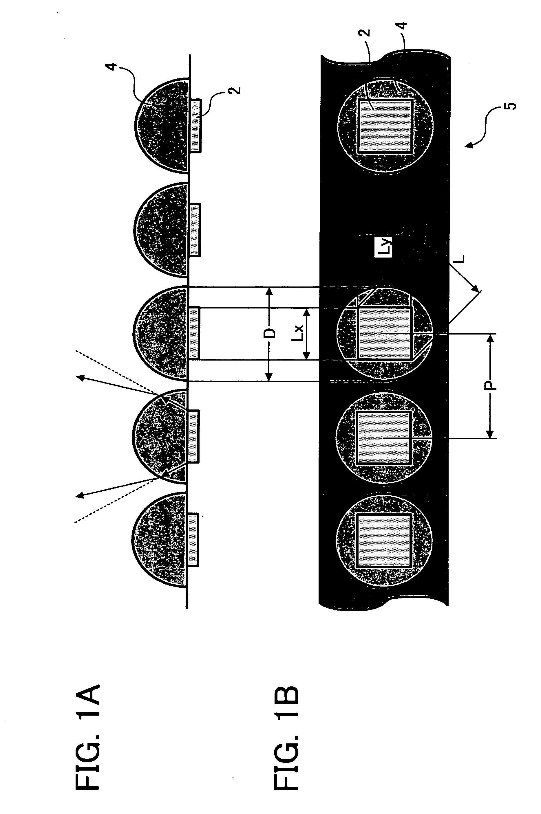
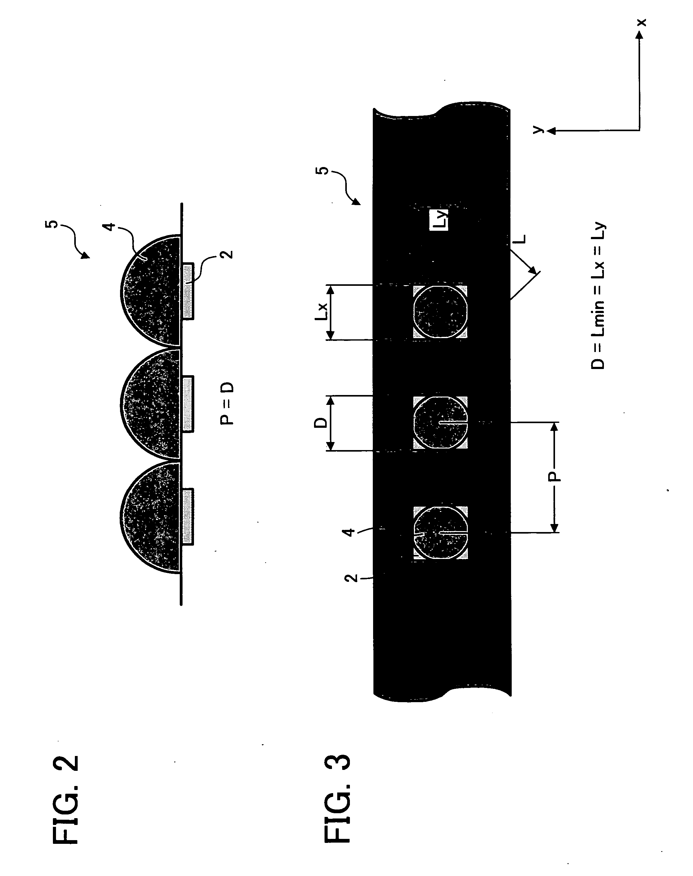
To achieve the foregoing and other objects, a light emitting array is provided including at least a plurality of light emitting elements, each of which is provided thereon with a microlens in one-to-one correspondence, in which the microlens is hemispherical in shape and separated from a microlens neighboring thereto.

In addition, the light emitting portion of the light emitting element is provided having the shape of rectangle and formed so as to satisfy the relational expression, Lmin≦D≦P, where Lmin is the length of the shorter side of the rectangle, P an alignment pitch of the light emitting elements, and D the diameter of the microlens.

The light emitting array disclosed herein may alternatively be formed with light emitting elements each having far-field emission angle characteristics of Lambert distribution.

The microlens included in the light emitting array may be formed of a transparent photoresist material on the light emitting elements formed in advance on a wafer.

...


PUM


Abstract

A light emitting array including at least a plurality of light emitting elements, each of which is provided thereon with a microlens in one-to-one correspondence. Light emitting portions of the light emitting element are provided having the shape of a rectangle and formed so as to satisfy the relational expression, Lmin≦D≦P, where Lmin is the length of the shorter side of the rectangle, P an alignment pitch of the light emitting elements, and D the diameter of microlens. In addition, light emitting elements are formed in line on a transparent thin film layer to satisfy the relationship, T1≦2·D2, where T1 is the thickness of the transparent thin film layer and D2 the diameter of each microlens. The light emitting array may suitably be included in the light source unit which is then incorporated into image forming apparatuses for forming mono-color or multiple-color images.

Description

BACKGROUND 1. Field of the Invention A light emitting array, and more specifically to light emitting arrays capable of reducing radiation angle of emerging light beams and obviating the generation of light flare, which is suitably adapted to the use in an optical writing unit and an image forming apparatus incorporating the writing unit. 2. Discussion of the Background In the course of recent developments in downsizing digital image forming apparatuses such as a digital duplication machine, a printer, a digital facsimile and so forth, more attention has been directed to the miniaturization of an optical writing unit in use for digital signal writing. Current methods for implementing optical writing are broadly divided into two classes. One class is a light scanning method in which a light beam emanated from a light source such as a semiconductor laser or other similar devices is scanned by a light deflecting unit to be formed subsequently as a beam spot through a scan imaging l...

Claims


Application Information

Patent Timeline
Patent Type & Authority Applications(United States)
IPC IPC(8): B41J2/44B41J2/45B41J2/455G02B3/00G02B5/00H01L25/075H01L33/08H01L33/20H01L33/58H04N1/036H05B33/00
CPCB41J2/451G02B3/0018H01L33/58H01L25/0753G02B3/005H01L2924/0002H01L2924/00
Inventor MASUDA, KOJISAKUMA, NOBUOITO, MASAHIRO
Owner RICOH KK
Why Eureka
Try Eureka