SnAgAu solder bumps, method of manufacturing the same, and method of bonding light emitting device using the same

a technology of light emitting devices and solder bumps, which is applied in the direction of soldering apparatus, semiconductor/solid-state device details, manufacturing tools, etc., can solve the problems of reducing the heat removal efficiency, and increasing the driving voltage of the light emitting device, so as to achieve the effect of increasing thermal stability

Active Publication Date: 2005-04-07
SAMSUNG ELECTRONICS CO LTD
View PDF13 Cites 34 Cited by
  • Summary
  • Abstract
  • Description
  • Claims
  • Application Information

AI Technical Summary

Benefits of technology

[0016] The present invention provides a solder bump which is formed at a lower temperature than a temperature at which the resistance of an elec...

Problems solved by technology

Additionally, when heat from the light emitting devices is removed via the wires, heat removal efficiency is decreased, ultimately leading to further increase in the driving vo...

Method used


Image

  • SnAgAu solder bumps, method of manufacturing the same, and method of bonding light emitting device using the same
  • SnAgAu solder bumps, method of manufacturing the same, and method of bonding light emitting device using the same
  • SnAgAu solder bumps, method of manufacturing the same, and method of bonding light emitting device using the same

Examples


Embodiment Construction

[0045] Hereinafter, a solder bump for bonding, a method of manufacturing the same, and a method of bonding a light emitting device using the solder bump, according to the present invention, will be described in detail by explaining embodiments of the invention with reference to the attached drawings. In the drawings, the thickness of layers and regions may be exaggerated for clarity.

[0046] Embodiments of the solder bump and the method of manufacturing the same will be described in the course of describing an embodiment of a method of bonding a light emitting device to a submount.

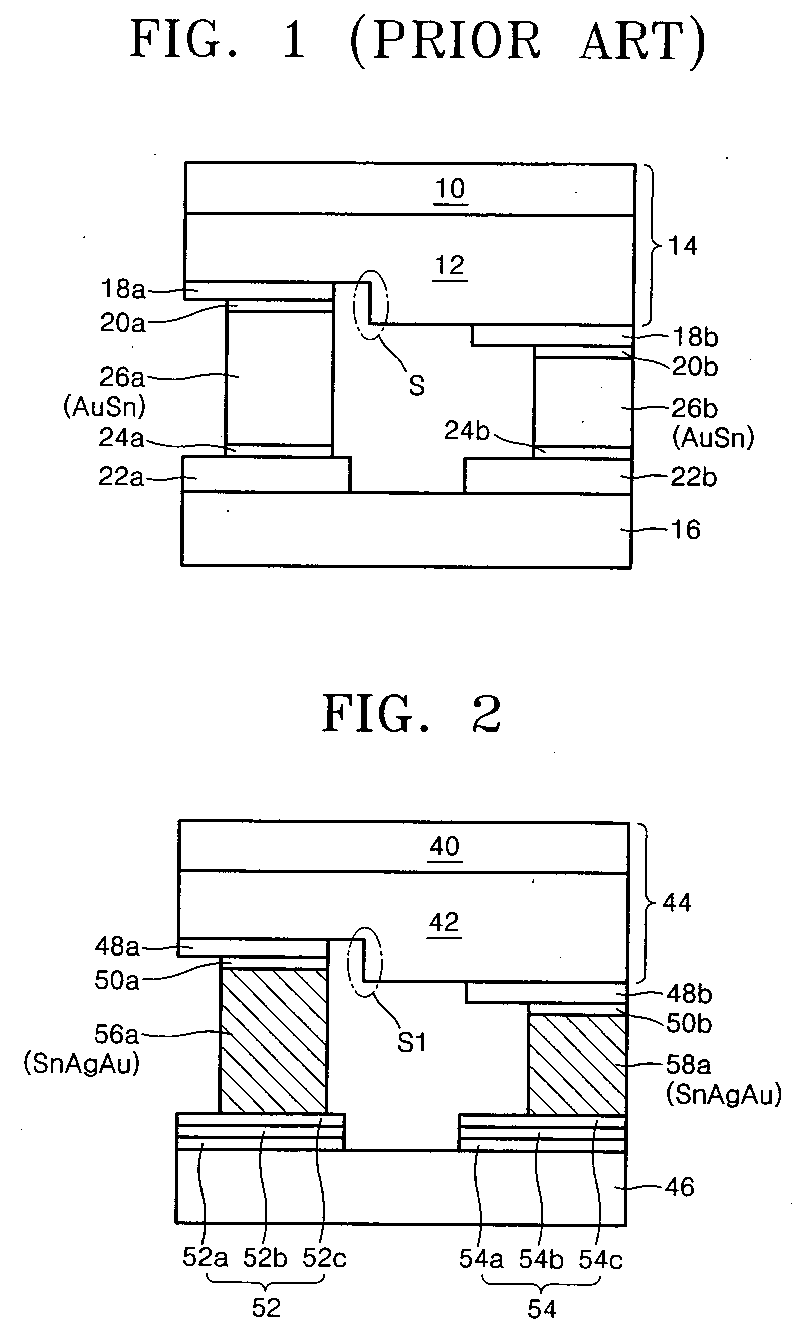
[0047] Referring to FIG. 2, reference numeral 44 denotes a light emitting device, such as a GaN compound semiconductor laser diode (LD) or a light emitting diode (LED). The light emitting device 44 includes a substrate 40 and a compound semiconductor layer 42 deposited on a lower surface of the substrate 40. The substrate 40 may be a high-resistance substrate such as a sapphire substrate or a transparent s...


PUM

PropertyMeasurementUnit
Temperatureaaaaaaaaaa
Fractionaaaaaaaaaa

Abstract

Provided are a solder bump, a method of manufacturing the same, and a method of bonding a light emitting device using the method of manufacturing the solder bump. In particular, the solder bump is formed of a compound including a first element through a third element, in which the first and third elements together form a compound having a plurality of intermediate phases and solidus lines.

Description

BACKGROUND OF THE INVENTION [0001] This application claims the priority of Korean Patent Application No. 2003-68321, filed on Oct. 1, 2003, in the Korean Intellectual Property Office, the disclosure of which is incorporated herein in its entirety by reference. [0002] 1. Field of the Invention [0003] The present invention relates to a bonding medium, a method of manufacturing the same, and a method of bonding two parts using the method of manufacturing the bonding medium, and more particularly, to a SnAgAu solder bump and a method of manufacturing the same, and a method of bonding a light emitting device using the solder bump. [0004] 2. Description of the Related Art [0005] Wire bonding has been widely used for bonding a light emitting device and a submount. The wire bonding between a light emitting device and a submount is performed not only to apply a driving voltage to the light emitting device, but also to remove heat generated by the light emitting device during its operation. [...

Claims


Application Information

Patent Timeline
IPC IPC(8): B23K35/00B23K35/26H01L21/60H01L23/485H01L33/32H01L33/62H01S5/022
CPCB23K35/001B23K35/262H01L24/10H01L24/81H01L33/62H01L2224/16H01L2224/06102H01L2924/01046H01L2924/01078H01L2924/01079H01L2924/01322H01L2924/12041H01L2224/0401H01L2224/81801H01L2924/12042H01L2924/00H01L21/60
Inventor CHOI, WON-KYOUNGCHAE, SU-HEEKWAK, JOON-SEOP
Owner SAMSUNG ELECTRONICS CO LTD
Why Eureka
Try Eureka