Sealing and protecting integrated circuit bonding pads

a bonding pad and integrated circuit technology, applied in the field of metalurgical systems, can solve the problems of bare copper bond pads that cannot be easily broken by a combination, weak bonding reliability of bonding wires, and inability to reliably attach bonding wires, etc., to achieve the effect of high reliability of finished ic assemblies

Inactive Publication Date: 2005-04-07
TEXAS INSTR INC
View PDF2 Cites 23 Cited by
  • Summary
  • Abstract
  • Description
  • Claims
  • Application Information

AI Technical Summary

Benefits of technology

[0010] The step of depositing a conductive seed layer can be preceded by a step of cleaning and etching the surface of the wafer, including the insulating layer and the exposed metallization, creating a fresh and activated surface. The seal provided by the prepared insulating layer and the deposited seed metal withstands operational thermomechanical stress.
[0013] Embodiments of the present invention are related to wire-bonded IC assemblies, semiconductor device packages, surface mount and chip-scale packages. It is a technical advantage that the invention offers a low-cost method of sealing the bond pad against moisture and delamination, and thus for protecting the integrated circuit against corrosion and stress-related contact failure. It is an additional technical advantage that the invention offers a methodology to smooth, stable interfaces of the gold wire ball and the modified bond pad, resulting in welds with strong metallic interdiffusion. Further technical advantages include the opportunity to scale the assembly to smaller dimensions, supporting the ongoing trend of IC miniaturization; and the absence of unwanted metals, supporting high reliability of the finished IC assemblies.

Problems solved by technology

For IC bond pads made of copper, the formation of thin copper(I)oxide films during the manufacturing process flow severely inhibits reliable attachment of bonding wires, especially for conventional gold-wire ball bonding.
In contrast to aluminum oxide films overlying metallic aluminum, copper oxide films overlying metallic copper cannot easily be broken by a combination of thermo-compression and ultrasonic energy applied in the bonding process.
As further difficulty, bare copper bond pads are susceptible to corrosion.
This process, though, has a number of drawbacks due to technical and cost issues.

Method used


Image

  • Sealing and protecting integrated circuit bonding pads
  • Sealing and protecting integrated circuit bonding pads
  • Sealing and protecting integrated circuit bonding pads

Examples


Embodiment Construction

[0025] The present invention is related to U.S. patent application Ser. No. 10 / 086,117, filed on Feb. 26, 2002 (Bojkov et al., “Waferlevel Method for Direct Bumping on Copper Pads in Integrated Circuits”).

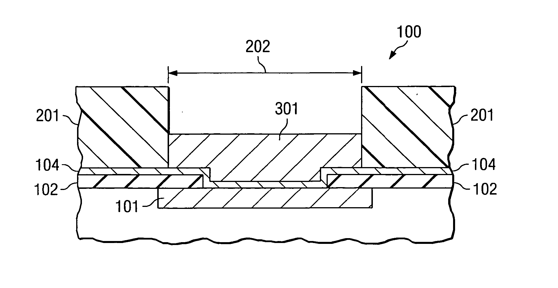
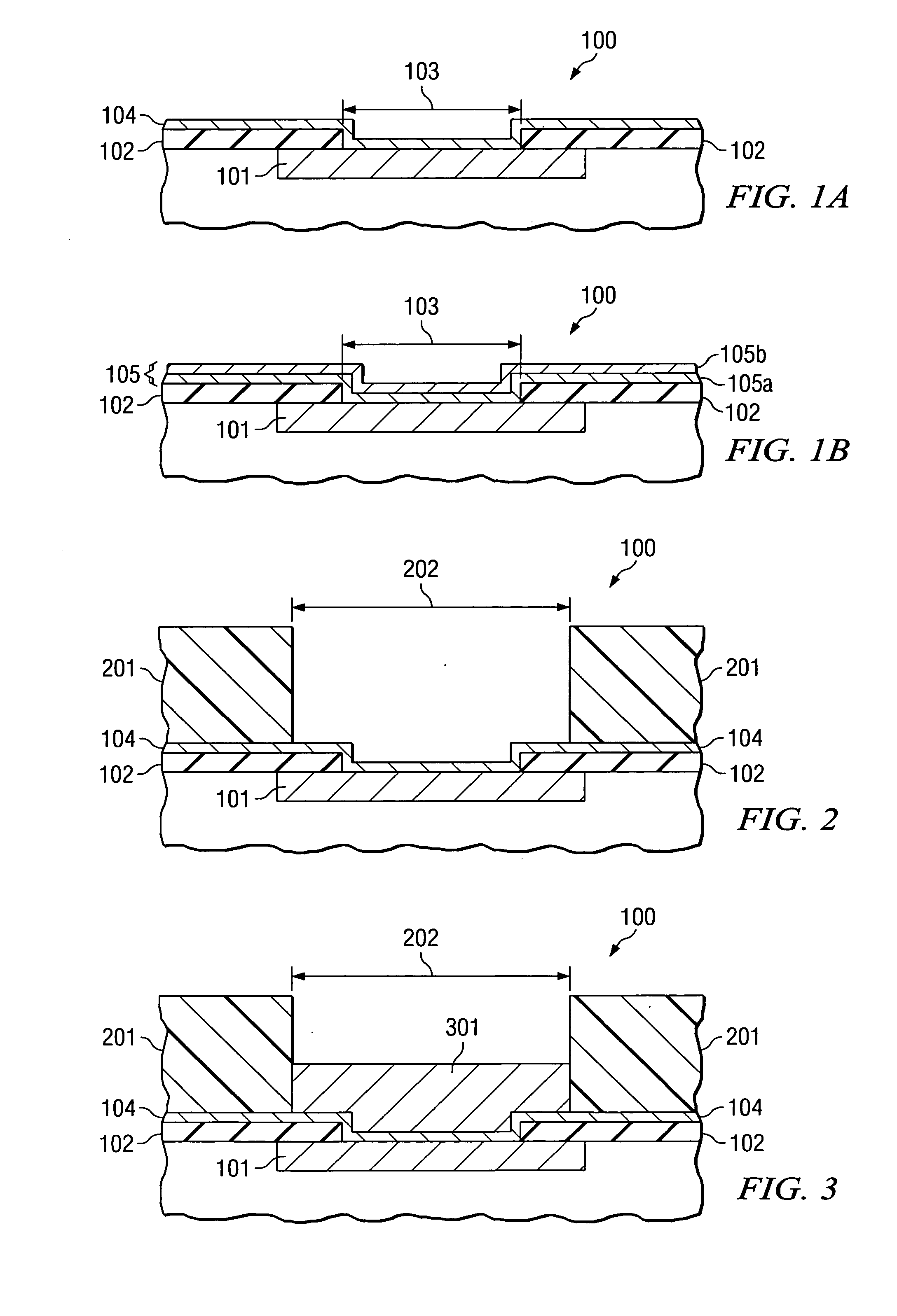
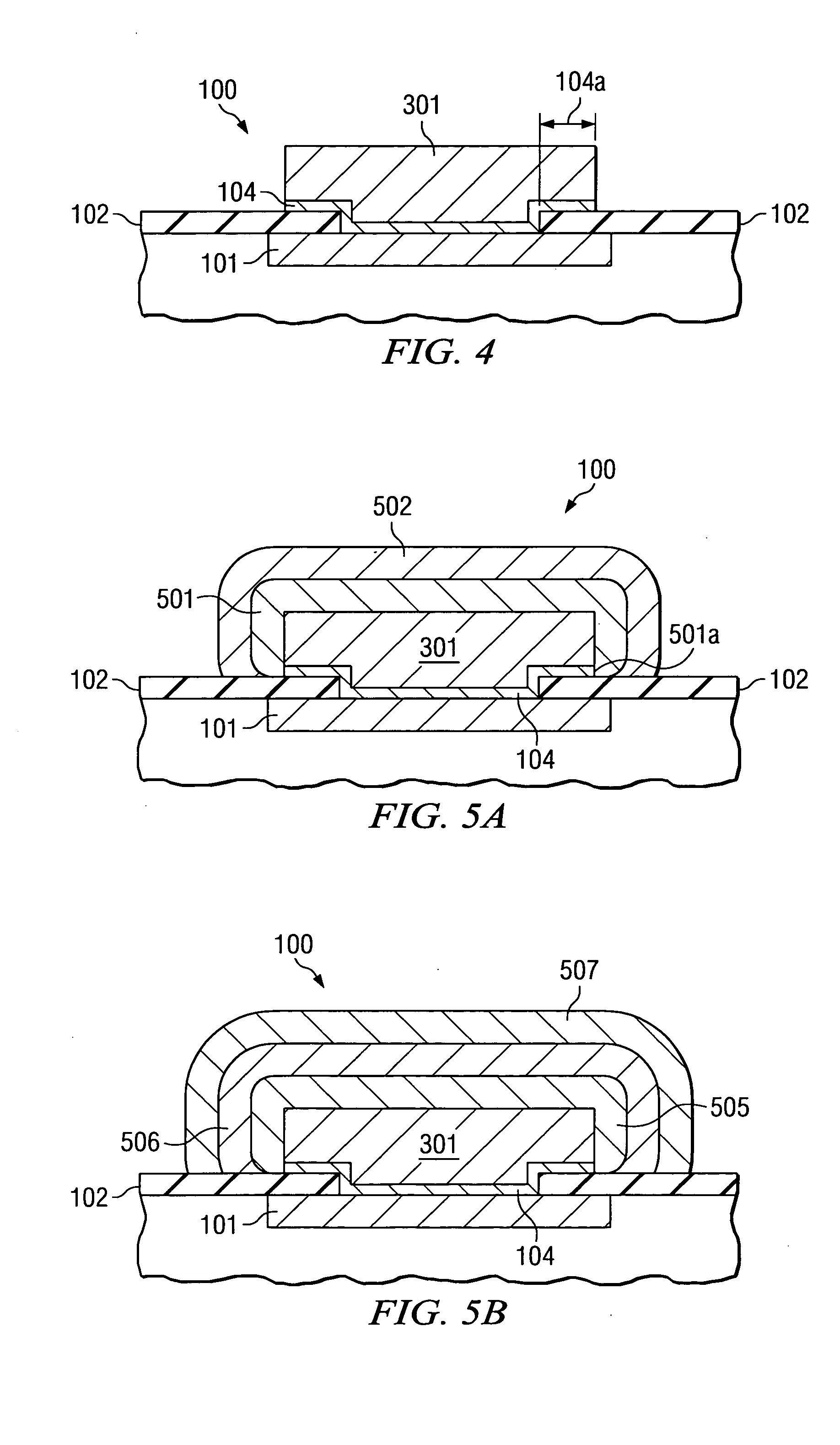
[0026]FIGS. 1A to 6B are schematic cross sections illustrating certain steps in the process flow for completing the fabrication of a bonding pad on an integrated circuit (IC) wafer. FIG. 1A shows schematically a portion of a semiconductor wafer, generally designated 100, having interconnections 101 and a protective overcoat 102. The semiconductor material is preferably silicon, but may alternatively be silicon germanium, gallium arsenide, or another III-V or II-IV semiconductor. The interconnection 101 is preferably copper; alternatively, aluminum or aluminum / copper alloy, or similar materials can be employed. The protective overcoat 102 is preferably silicon nitride, but may alternatively be silicon oxynitride, silicon carbide, silicon dioxide, or a polymer such as polyimide, for...


PUM


Abstract

A metal structure (600) for a bonding pad on integrated circuit wafers, which have interconnecting metallization (101) protected by an insulating layer (102) and selectively exposed by windows in the insulating layer. The structure comprises a patterned seed metal layer (104) positioned on the interconnecting metallization exposed by the window so that the seed metal establishes ohmic contact to the metallization as well as a practically impenetrable seal of the interface between the seed metal and the insulating layer. Further, a metal stud (301) is formed on the seed metal and aligned with the window. The metal stud is conformally covered by a barrier metal layer (501) and an outermost bondable metal layer (502).

Description

FIELD OF THE INVENTION [0001] The present invention is related in general to the field of metallurgical systems with application to electronic systems and semiconductor devices and more specifically to methods for sealing and protecting integrated circuit bonding pads. DESCRIPTION OF THE RELATED ART [0002] It is a continuing trend in the semiconductor industry to miniaturize integrated circuits (ICs). As a consequence of this trend, the RC time constant of the interconnection between active circuit elements increasingly dominates the achievable IC speed-power product. Consequently, there is a strong need to replace the relatively high impedance of the interconnecting aluminum metallization by the lower impedance of metals such as copper. [0003] For IC bond pads made of copper, the formation of thin copper(I)oxide films during the manufacturing process flow severely inhibits reliable attachment of bonding wires, especially for conventional gold-wire ball bonding. In contrast to alumi...

Claims


Application Information

Patent Timeline
Patent Type & Authority Applications(United States)
IPC IPC(8): H01L23/485
CPCH01L24/05H01L24/45H01L24/48H01L2224/04042H01L2224/05083H01L2224/05111H01L2224/05116H01L2224/05118H01L2224/05123H01L2224/05124H01L2224/05147H01L2224/05155H01L2224/05157H01L2224/0516H01L2224/05164H01L2224/05639H01L2224/05644H01L2224/05655H01L2224/05664H01L2224/05669H01L2224/45124H01L2224/45139H01L2224/45144H01L2224/45147H01L2224/48463H01L2224/85205H01L2924/01002H01L2924/01007H01L2924/01012H01L2924/01013H01L2924/01014H01L2924/01018H01L2924/01022H01L2924/01027H01L2924/01028H01L2924/01029H01L2924/0103H01L2924/01031H01L2924/01032H01L2924/01042H01L2924/01046H01L2924/01047H01L2924/0105H01L2924/01073H01L2924/01074H01L2924/01075H01L2924/01078H01L2924/01079H01L2924/01082H01L2924/05042H01L2924/10253H01L2924/14H01L2924/3011H01L2924/3025H01L2924/01023H01L2924/01024H01L2924/01033H01L2924/01076H01L2224/48644H01L2224/48655H01L2224/48664H01L2224/48669H01L2224/48839H01L2224/48844H01L2224/48855H01L2224/48864H01L2224/48639H01L2224/48739H01L2224/48755H01L2224/48764H01L2224/48769H01L2224/05556H01L2924/00014H01L2924/00H01L2224/48869H01L2224/48744H01L2224/45014H01L2924/10271H01L2924/1032H01L2924/10329H01L2924/1037H01L2924/206H01L2224/45015H01L2924/207
Inventor BOJKOV, CHRISTO P.KRUMNOW, MICHAEL L.
Owner TEXAS INSTR INC
Why Eureka
Try Eureka