Mount for Semiconductor Devices Using Conformable Conductive Layers, and Method

a technology of conformable conductive layers and semiconductor devices, which is applied in the direction of lasers, laser construction details, semiconductor lasers, etc., can solve the problems of brittle laser materials, remarkably small size of led and laser diodes, and mechanical approach that has not proved practical with semiconductor devices such as laser diodes, etc., and achieves excellent heat conduction away and simple manufacturing.

Inactive Publication Date: 2013-03-07
GROVE ROBERT E
View PDF4 Cites 24 Cited by
  • Summary
  • Abstract
  • Description
  • Claims
  • Application Information

AI Technical Summary

Benefits of technology

The present invention provides improved heat conduction for semiconductor devices through the use of compressible thermally conductive graphite sheets with a spacer between them. This results in optical performance similar to that achieved with laser diodes soldered to a heatsink while being simpler and cheaper to manufacture. A multilayer sandwich can be formed with multiple slots for semiconductor devices, providing reliable and cost-effective assembly.

Problems solved by technology

Both LED's and laser diodes are of remarkably small size given the amount of light these devices can emit, the amount of power they consume, and the amount of heat that they generate.
The mechanical approach has not proved practical with semiconductor devices such as laser diodes, for two reasons.
First, the laser itself has no casing or housing, and the laser material is quite brittle.
Thus, the pressure necessary to achieve good thermal conductivity using a hard heat sink surface can result in cracking of the semiconductor device, either immediately or during use.
Secondly, while thermal grease can help achieve high thermal conductivity with a lighter pressure, the grease tends to migrate toward the optical surfaces of the laser diode, resulting in permanent damage to the laser.
However, this approach has its own inherent drawbacks, especially for laser diodes, which are typically fabricated out of gallium arsenide or indium phosphide.
A simple soldering to a copper heatsink routinely fails due to the difference in the thermal expansion coefficient between the laser diode material and the heatsink material.
To overcome this problem, more difficult to fabricate (and expensive) heatsink material must be used, having a comparable thermal expansion coefficient.
Because the thermal expansion coefficient of solder is also not perfectly matched to that of the semiconductor, it too places stresses on the laser diode.
A related challenge for soldering is that the laser diode has an output facet coating consisting of a partially-transmitting, multilayer dielectric material, and a highly reflective coating on the rear laser facet.
Both of these optical surfaces must be completely undisturbed during the soldering process, or the laser will likely fail.
Thus, many fluxes that might typically be used to remove oxides during the soldering process cannot be used.
In addition, it is desirable to subject laser diodes to minimal temperature rise during soldering, but low melting-point solders such as indium and its alloys do not generally “wet” surfaces as well as higher temperature solders.
Still further, the solder must be in intimate contact with the entire length of the laser stripe; if it is not, the region without contact becomes catastrophically hot.
Unfortunately, when the optical coating is deposited onto the output facet of the laser diode chip, some of the coating material may get inadvertently deposited on the P-side of the chip and prevent the solder from bonding to the chip in that area.
This typically results in infant failure of the chip.

Method used


Image

  • Mount for Semiconductor Devices Using Conformable Conductive Layers, and Method
  • Mount for Semiconductor Devices Using Conformable Conductive Layers, and Method
  • Mount for Semiconductor Devices Using Conformable Conductive Layers, and Method

Examples


Embodiment Construction

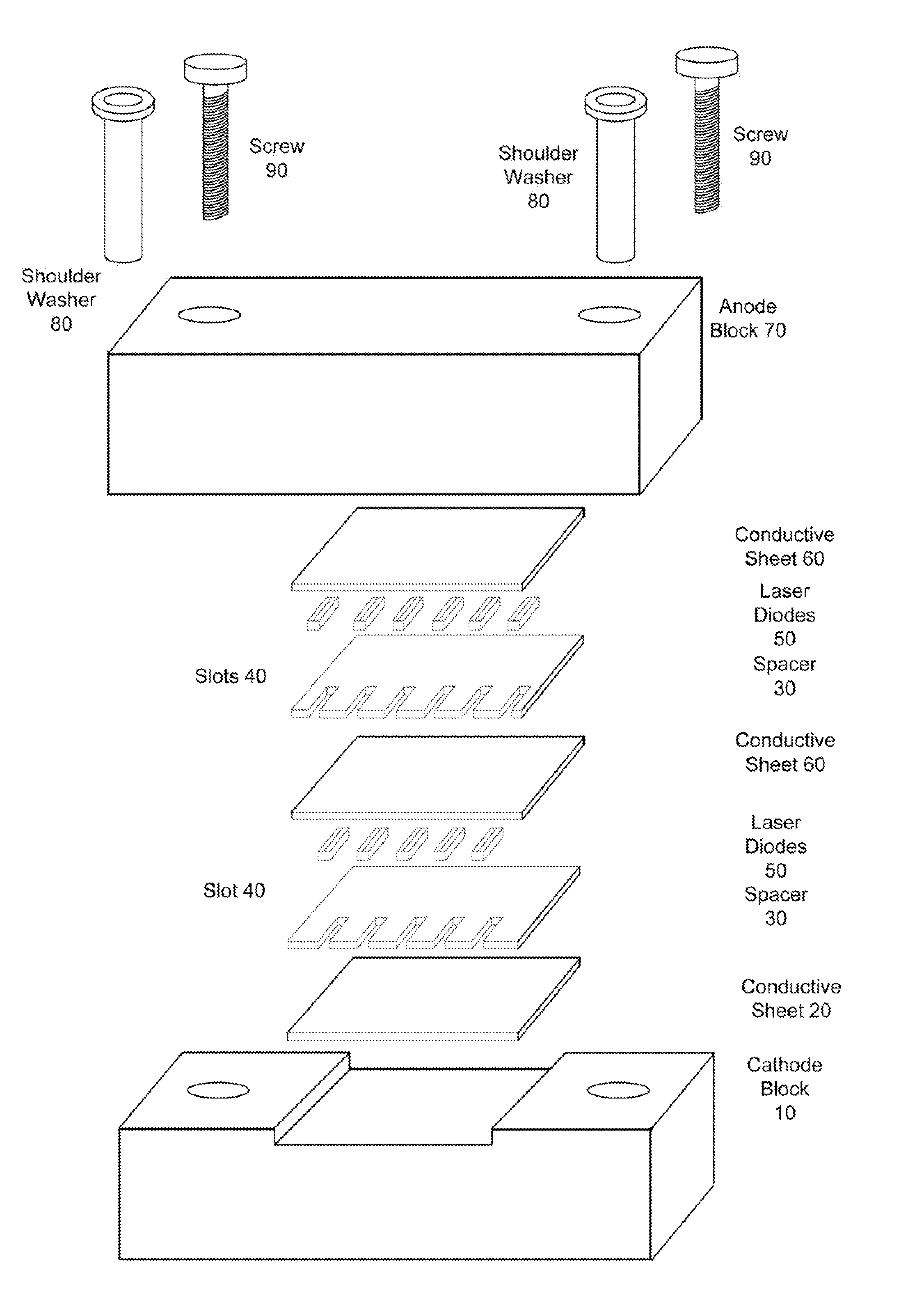
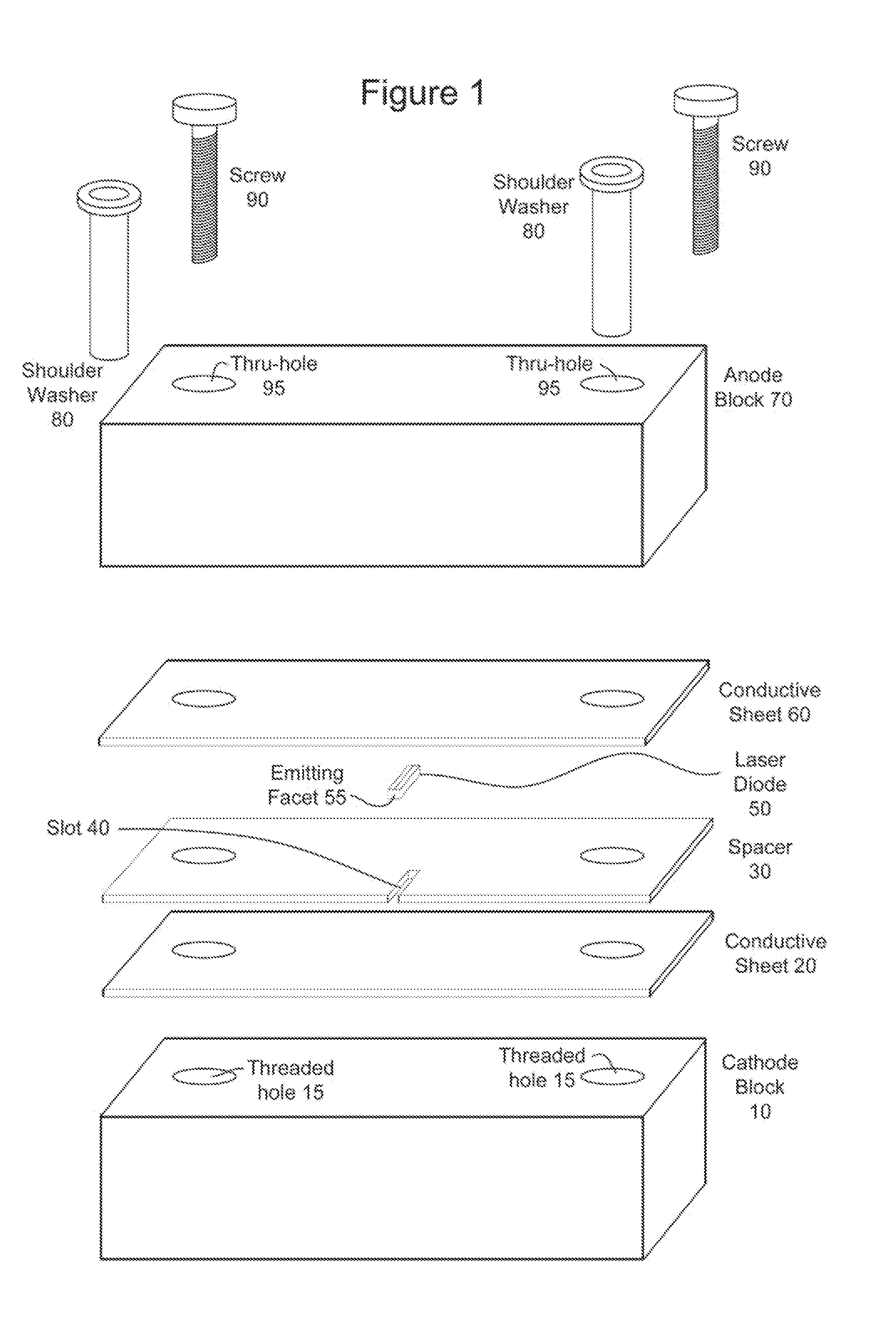
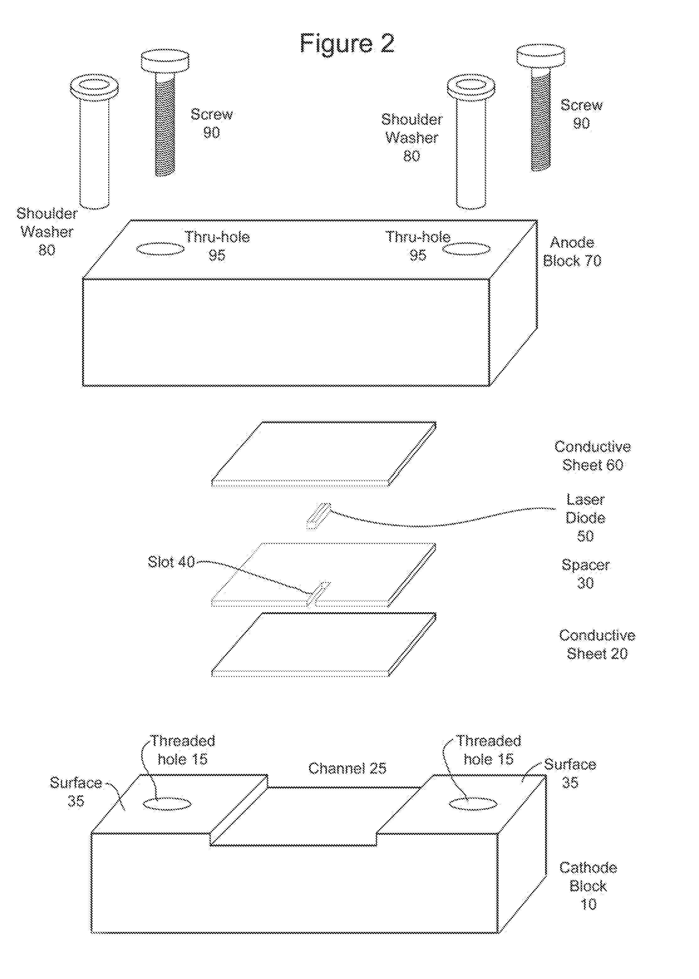
[0022]Referring to FIG. 1, an embodiment of a device in accordance with the invention is shown in an exploded view. In such an embodiment, the device can be of generally rectangular shape, of dimensions nominally 0.5 inch wide by 0.25 inch deep by 0.25 inch in thickness. It will be appreciated that these dimensions and shapes are exemplary only, and are largely a matter of design choice. Thus, the dimensions and shapes shown and described herein are not intended to be limiting. For example, the entire device could be made much smaller by simply utilizing screws smaller than the 0-80 size contemplated in the drawing, or by using glue as discussed in connection with the embodiment of FIG. 4. Similarly, the shape can be altered to any convenient form, as long as sufficient compression is provided to ensure reliable mechanical placement as well as thermal and electrical conductivity among the various components, together with sufficient heat removal.

[0023]In the embodiment shown in FIG....


PUM


Abstract

Mount for semiconductor laser devices comprises thermally conductive anode and cathode blocks on either side of semiconductor laser device such as laser diode. Interposed between at least the anode block and the anode of the semiconductor laser device is a sheet of conformable electrically conductive material with high thermal conductivity such as pyrolytic highly-oriented graphite. In some embodiments, a second sheet of such electrically and thermally conductive conformable material is interposed between the cathode of the semiconductor laser device and the cathode block. The semiconductor laser device can be either a single laser diode or a diode bar having a plurality of emitters. A thermally conductive, but electrically insulating, spacer of essentially the same thickness as the laser diode or bar surrounds the diode or bar to prevent mechanical damage while still permitting the conformable material to be maintained in a compressed state and directing current through the laser device.

Description

RELATED APPLICATION[0001]This application is a conversion of U.S. Patent Application Ser. No. 61 / 528,747, filed Aug. 29, 2011, and a divisional of U.S. patent application Ser. No. 13 / 476,762, filed May 21, 2012, both of which are incorporated herein by reference, and claims the benefit of each of the foregoing applications.FIELD OF THE INVENTION[0002]This invention relates generally to methods and apparata for mounting semiconductor devices, and more particularly relates to methods and apparata for mounting of light-emitting semiconductor devices such as laser diodes and the like.BACKGROUND[0003]Light-emitting semiconductor devices have been developed over the past several decades to emit either incoherent light (devices referred to as “LED's”) or coherent light (referred to as “laser diodes” or “diode lasers”.) A common attribute of both LED's and laser diodes is a pair of electrically conducting surfaces, serving as the anode and cathode of the device, through which an electrical ...

Claims


Application Information

Patent Timeline
Patent Type & Authority Applications(United States)
IPC IPC(8): H01S5/024H01L21/50H01S5/023H01S5/0233
CPCH01S5/02461H01S5/02476H01S5/02236H01S5/02264H01S5/02365H01S5/023H01S5/0233H01S5/0235H01S5/02469H01S5/024H01S3/0405
Inventor GROVE, ROBERT E.
Owner GROVE ROBERT E
Why Eureka
Try Eureka