

Pb-free solder alloy, and solder material and solder joint using same
a solder alloy and solder joint technology, applied in the direction of welding/cutting media/materials, manufacturing tools, soldering apparatus, etc., can solve the problems of parts melting point exceeding heat resistance temperature of parts, difficult to increase heat resistance of corresponding parts, and possible damage to parts, etc., to achieve the effect of improving the reliability of solder joints
- Summary
- Abstract
- Description
- Claims
- Application Information
AI Technical Summary
Benefits of technology
Problems solved by technology
Method used
Image

Examples
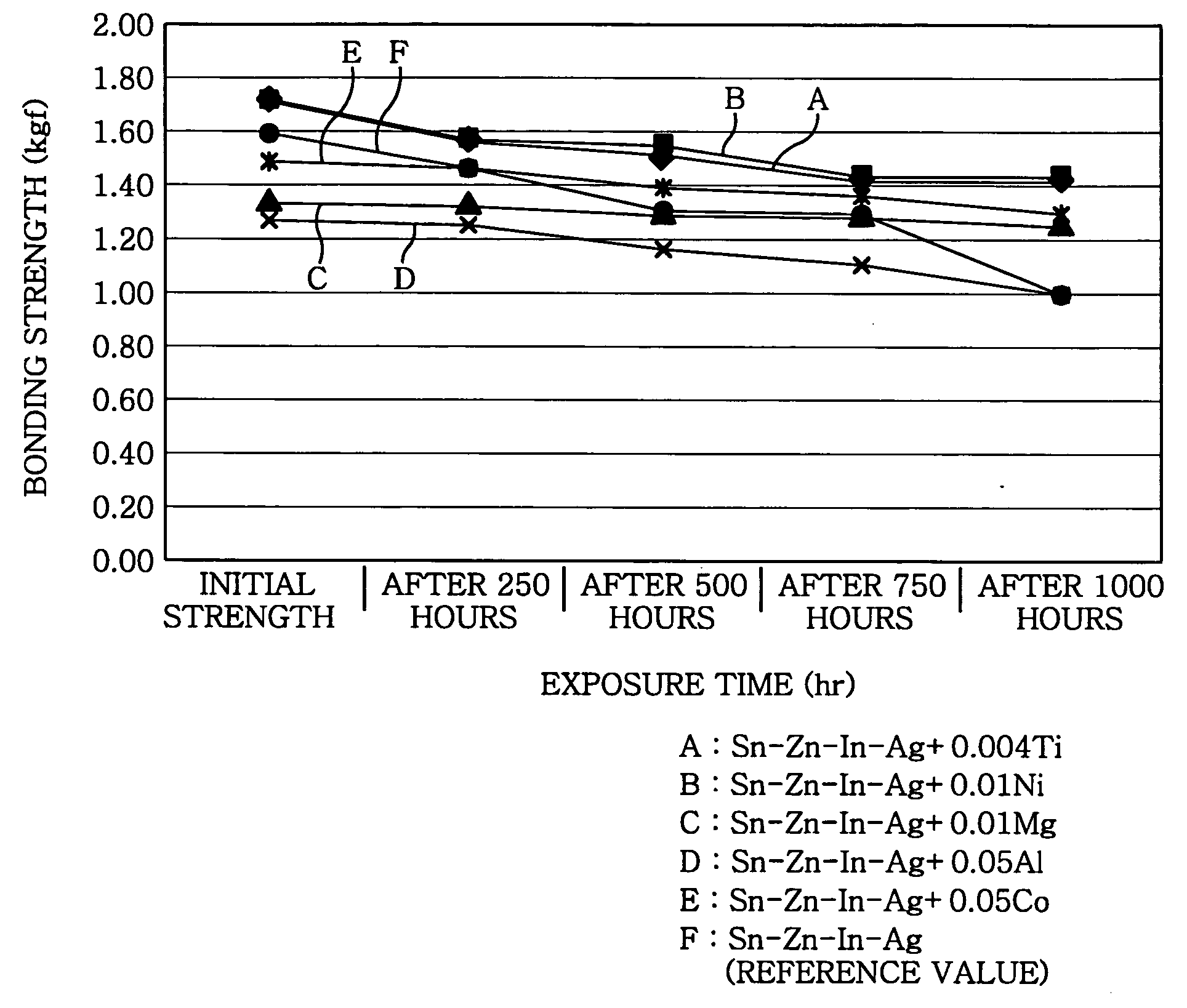
example 1
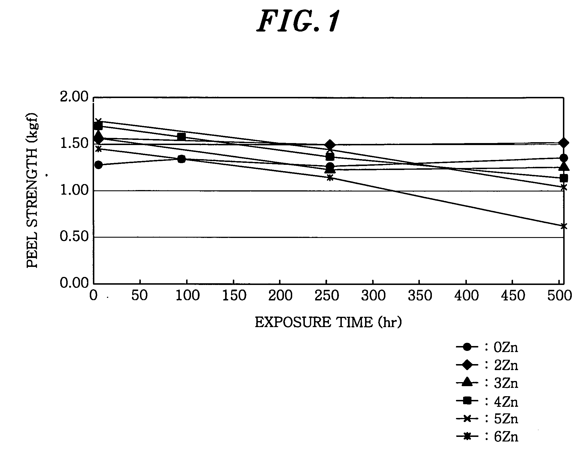
[0049] In Example 1, a peel strength of a joint having, in weight, 3% In and 0-6% Zn (the remaining portion was Sn) was measured, with respect to a variation of a bonding strength when exposed to an environment of the high temperature and high humidity.
[0050] First, a solder alloy, which was mixed to have a predetermined composition, of about 1 kg was held at 230° C. And then, QFP (Quad Flat Package) parts of 0.65 mm in pitch and 100 pins are fixed to a Cu-attached glass epoxy PCB by using an adhesive. This specimen was applied to a flux, and then, subjected to soldering by dipping into the solder. A soldered article was washed with acetone by using a microwave washing machine, so that residuals of the flux were removed. A soldered PCB specimen after being washed was put into a hygro-thermostat (constant temperature and humidity oven) kept at 85° C. and 85% RH, and then, a peeling strength of a lead bonding strength was measured for every 250 hours.
[0051]FIG. 1 shows a variation o...
example 2
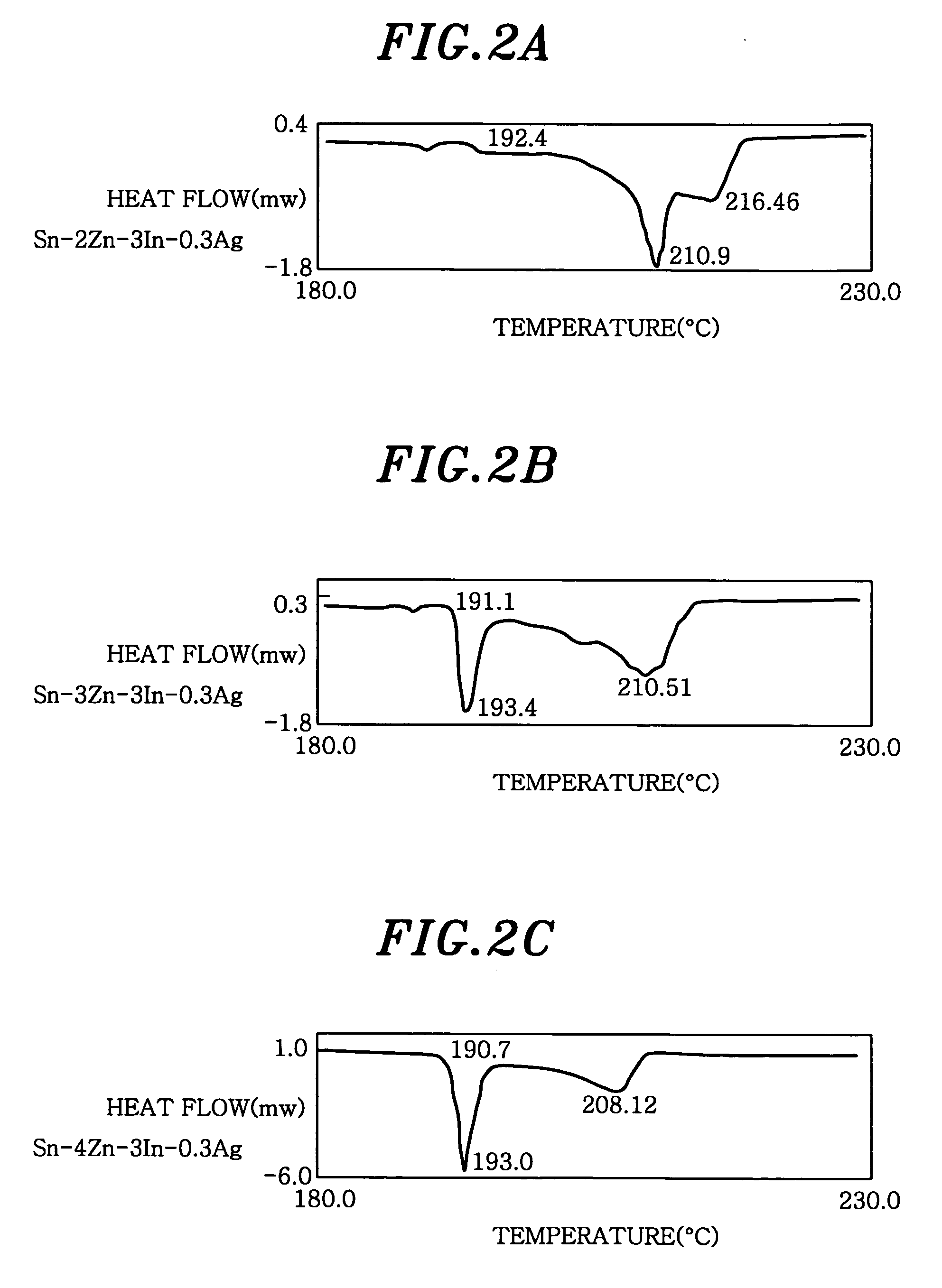
[0055] Example 2 was carried out for observing a structure, in case when a small amount of Ag is added to an Sn-4Zn-3In. Each solder having, in weight, 4% Zn, 3% In, 0.1-0.5% Ag, and the balance Sn of about 0.6 g was melted on a ceramic plate to form a sphere shape, and in that state, cooled in the air. A section of each solder particle was polished and observed by using scanning electron microscope (SEM). The results were described in FIGS. 3A to 3C.
[0056] As is known from FIGS. 3A to 3C, needle like Zn phases decrease as the Ag concentration increases. Further, it can be noted that spheroidal Zn—Ag phases increase in FIGS. 3B and 3C. Still further, a fine structure of the solder is confirmed. Zn phases are finely dispersed, so that a connection between the Zn phases disappears. Accordingly, oxidation of Zn, which causes to lower a bonding strength, does not spread towards an inside of the solder, and lowering of a bonding strength under the condition of the high temperature and h...
example 3
[0058] In Example 3, a variation of an electrochemical corrosion potential would be explained, in case when a small amount of Ag is added to the Sn-4Zn-3In.
[0059] Each solder having, in weight, 4% Zn, 3% In, 0-0.5% Ag, and the balance Sn was prepared with a bar shape having a cross section of 5 mm×5 mm. A surface of the bar-shaped specimen was polished with water resistance polishing paper of 1200 mesh, and then, subjected to buffing by using Al2O3 suspension. Subsequently, the specimen was immersed into a 3.5 wt. % NaCl water solution at 25° C. Further, by using a standard electrode employing a silver electrode, a silver chloride electrode, and a saturated KCl water solution, an electromotive force difference, which is generated between Ag of the standard electrode and the solder specimen, was measured. The result was shown in FIG. 4. Still further, as a reference sample, an electrochemical corrosion potential of the Sn-3In solder not containing Zn was described.
[0060] As is know...
PUM
| Property | Measurement | Unit |
|---|---|---|
| melting point | aaaaa | aaaaa |
| melting points | aaaaa | aaaaa |
| melting points | aaaaa | aaaaa |
Abstract
Description
Claims
Application Information