Tunable thin film capacitor

a thin film capacitor and capacitor technology, applied in the direction of capacitors, semiconductor devices, transistors, etc., can solve the problems of inability to obtain a sufficiently wide variable range, inability to stabilize the dielectric constant of the dielectric layer, and inability to achieve sufficient dielectric constant control, etc., to achieve short time, low cost, and efficient fabrication

Inactive Publication Date: 2005-04-21
KYOCERA CORP
View PDF2 Cites 142 Cited by
  • Summary
  • Abstract
  • Description
  • Claims
  • Application Information

AI Technical Summary

Benefits of technology

[0041] Still another object of the invention is to provide a tunable thin film capacitor constituted such that the dielectric layer does not peel off, and in addition, the resistance in the upper electrode layer of the capacitance can be easily lowered, and, even in the case a relatively high capacitance-controlling voltage is applied to the dielectric layer, the capacitor can withstand it.
[0164] Particularly, the surface of the dielectric layer with a low dielectric constant is uneven or projected and depressed due to the crystal grain diameters of the oxide grains containing Ba and Sr. As a result, the upper electrode layer formed on the thin film dielectric layer closely adheres to the thin film dielectric layer so as to tightly engage with each other. Accordingly, the upper electrode layer is hard to peel off, and further, even in case that the thickness of the upper electrode layer is increased, the upper electrode layer is still hard to peel off, as a result of which the electrode loss can be reduced.

Problems solved by technology

This external control voltage is, for example, ten to several tens of volts, but this external control voltage is, actually, hard to be uniformly applied to the capacitance-producing region; and thus, it is difficult to stabilize the dielectric constant of the dielectric layer 163 to a predetermined value.
In other words, in the same capacitance-producing region, a distribution of potential takes place, resulting in the problem that the sufficient dielectric constant control, i.e., a sufficiently wide variable range, cannot be obtained; due to this, there has been the problem that a capacitance corresponding to the external voltage cannot be obtained as according to the specifications.
The existence of this hollow structure results in giving a large restriction when the capacitor is mounted on a mother board and in lacking in reliability.
Further, as for the method of manufacturing the upper electrode layer 164, an organic resist is used for the formation of the air bridge 165, and thus, a manufacturing method deviating from the thin film technology must be used, so that the manufacturing steps become very complicated.
In practice, however, it is difficult to increase the thickness of the lower electrode layer 162.
Thus, a portion of the upper electrode layer 164 is positioned in the air like a bonding air, so that it is very difficult to actually mount the capacitor onto a mother board or the like; and thus, the known tunable thin film capacitor could hardly be put to practical use.
In order to reduce the capacitance of the capacitor, it is necessary to decrease the area of the capacitance-producing region comprised of the thin film dielectric layer sandwiched between the lower electrode layer and the upper electrode layer, but, by decreasing the area of the capacitor, a step that deteriorates the leakage characteristic is formed in the dielectric portion constituting the capacitor, and the accuracy in positional matching becomes hard to achieve at the manufacturing steps, thus resulting in a fall in manufacturing yield.
In order to reduce the loss due to the lower electrode layer and the upper electrode layer, it is necessary to use a metal with a low resistivity; gold, silver, copper, aluminum, etc. are efficient, but, in the case of these metals, there is the possibility that there may be caused the problem that these metals are each oxidized at a high temperature during the manufacturing steps, the film quality thereof is deteriorated, the metals are chemically reacted with the dielectric layer.
For example, in the case of an electrode comprised of gold, the smoothness of the electrode is deteriorated at a high temperature, which will cause the short-circuiting of the capacitor.
However, there has been caused the problem that the high-melting metal material is low in conductivity as compared with gold or the like, and, in particular, the electrode loss cannot be reduced in a high frequency region higher than 1 GHz.
Further, in case that platinum is used as the material of the reaction-preventing layer, there has also been caused the problem that the thermal stress of the reaction-preventing layer is large, so that the reaction-preventing layer is apt to peel off from the interface between the lower electrode layer and the support substrate due to the change in temperature during the manufacturing steps.
Further, in case that gold is used as the conductive layer of the lower electrode layer, the film quality is markedly deteriorated due to the high temperature during the manufacturing steps, and thus, there have been caused problems such as the problem that the capacitor is short-circuited and the problem that the leakage current becomes large.
Further, Ti, Cr, and the like are easy to react with BST and PZT that are general dielectric materials, so that, in case that these metals are used as adherent layers, there is the possibility that the characteristic of the dielectric may be deteriorated at the time of a process using a high temperature.
Further, due to the curved shape which is peculiar to the air bridge structure, there was caused the problem that the self-inductance L was large, so that the self-resonant frequency, defined by the condition: fo=½ (LC)1 / 2 wherein C represents a static capacitance, was small, and thus, the operating frequency was limited to a low frequency region.
In the varactor diode, its loss is increased at high frequencies, and, in the case of using a low voltage, the depletion layer becomes thin, and the leakage current increases; and thus, the varactor diode theoretically ceases to function as a capacitor, so that it is difficult to make the varactor diode compatible with a high-frequency circuit (compatibility with the high-frequency operation).
Normally, in the case of forming a thin metal film, sputtering is performed in an atmosphere comprising only an Ar gas, but, in the case of using ceramics, the elimination of oxygen takes place at the time of film-forming deposition, as a result of which the oxygen concentration of the fabricated dielectric layer becomes less than that of the stoichiometric composition, and a large amount of lattice defects of oxygen are produced.
However, the method of suppressing the deterioration in dielectric loss due to the lattice defects of oxygen or the production itself of lattice defects of oxygen is problematic in that the method requires a heat treatment extending over a long time after the sputtering and thus poor in efficiency from the viewpoint of a method of fabricating variable capacitance capacitors with an enhanced productivity; and thus, variable capacitance capacitors cannot be fabricated with low costs.
However, at the steps of manufacturing a thin film capacitor, the electrodes are formed by the thin film technique and the photolithography method, so that the manufacturing steps become complicated.
Further, there is the problem that, in case the electrodes are made too thick, the electrodes peel off from the surfaces to which they are to adhere.

Method used


Image

  • Tunable thin film capacitor
  • Tunable thin film capacitor
  • Tunable thin film capacitor

Examples


embodiment 1

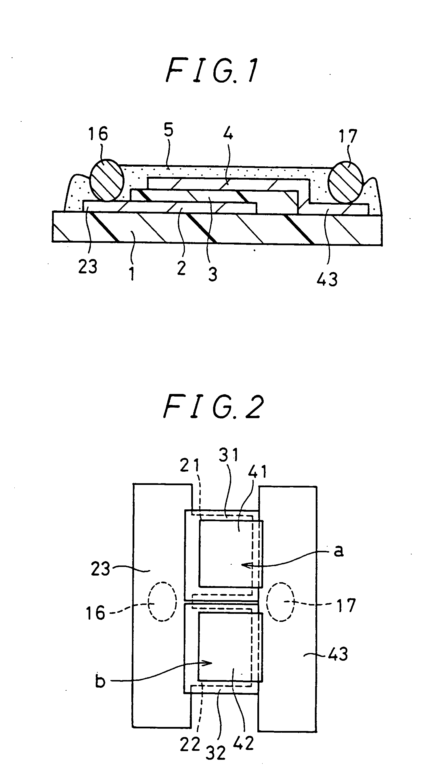
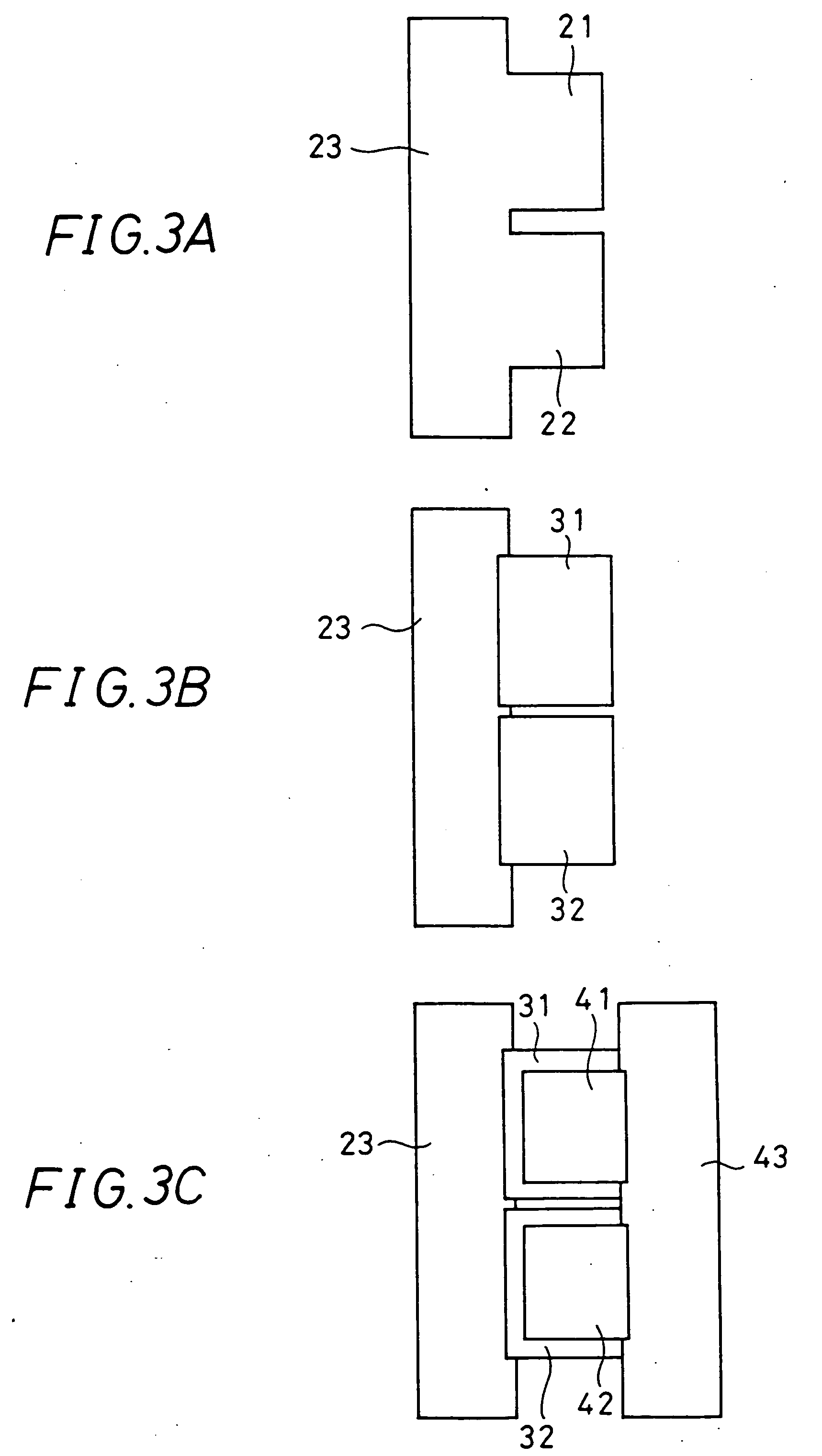
[0207] The tunable thin film capacitor shown in FIG. 2 was fabricated. On sapphire used as the support substrate 1, a substratum Ti layer and an upper-laid Au layer were formed as the lower electrode layers 21, 22 by the sputtering process. The substratum Ti layer is for enhancing the adherence between the support substrate 1 and the upper-laid Au layer, and, as for the thickness, the thickness of Ti was set to 0.05 μm, and the thickness of Au was set to 1 μm. This substratum electrode layer was processed by the photolithography technology to form the lower electrode layers 21, 22 and the lower terminal electrode layer 23 shown in FIG. 2. More specifically, a resist was applied to a predetermined shape and patterned by wet etching.

[0208] Subsequently, for the formation of the thin film dielectric layers 31, 32, (Ba, Sr) TiO3 was deposited to a thickness of 1 μm by the sputtering process, and, by the photolithography and wet etching processes, the thin film dielectric layers 31, 32 ...

embodiment 2

[0249] On a ceramic substrate, a TiO2 layer with a thickness of 20 nm and an Au film with a thickness of 0.3 μm were formed by the sputtering process under the condition that the deposition temperature be 250° C., and the Ar gas pressure be 5 mTorr. This Au film was processed to a predetermined shape by wet etching, whereby the first thin film substratum conductor layer 61 and the second thin film substratum conductor layer 62, which were both comprised of Au, could be formed.

[0250] Next, on the first thin film substratum conductor layer 61 and the second thin film substratum conductor layer 62 formed by Au thus formed, a thin film dielectric layer with a thickness of 0.15 μm was formed by processing a dielectric material represented by (Ba1-xSrx) TiO3 (wherein 02 gas pressure be 18 mTorr. Subsequently, by etching this thin film dielectric layer, the thin film dielectric layer 3 having a predetermined shape and covering the separation portion X between the first thin film substratu...

embodiment 3

[0275] In this tunable thin film capacitor, for example the thin film substratum conductor layers 82a, 82b, the thin film dielectric layer 3, and the thin film superstratum conductor layers 84a, 84b were successively formed on a ceramic substrate 1, respectively.

[0276] First, on the ceramic substrate 1 with a thickness of, e.g., 0.3 mm, a Pt film with a thickness of 0.3 μm was formed by the sputtering process under the condition that the deposition temperature be 600° C., and the Ar gas pressure be 10 mTorr. This Pt film was processed to a predetermined shape by dry etching, whereby the first and second thin film substratum conductor layers 82a, 82b made of Pt were formed.

[0277] Next, extending over the first thin film substratum conductor layer 82a and the second thin film substratum conductor layer 82b, both being comprised of Pt, the thin film dielectric layer 3 with a thickness of 0.3 μm was formed by sputtering a dielectric material represented by (Ba1-xSrx) TiO3 (wherein, 02...


PUM


Abstract

It is an object of the invention to provide a variable capacitor constituted such that, even when an external control voltage is applied, a stable dielectric constant of the dielectric layer can be obtained. A variable capacitor constituted such that a dielectric layer whose dielectric constant is changed by the application of an external voltage is held between an upper electrode layer and a lower electrode layer, wherein a plurality of capacitance-producing regions a, b are connected to each other.

Description

BACKGROUND OF THE INVENTION [0001] 1. Field of the Invention [0002] The present invention relates to a tunable thin film capacitor with a thin film dielectric layer whose dielectric constant is changed by the voltage applied across a lower electrode layer and an upper electrode layer. [0003] 2. Description of the Related Art [0004] It is so far known that a strontium titanate (SrTiO3) thin film that is a paraelectric substance or a strontium barium titanate (Ba, Sr) TiO3 thin film that is a ferroelectric substance exhibits a non-linear change in the dielectric constant thereof upon application of a predetermined voltage to the dielectric thin film thereof (A. Walkenhorst et al., Appl. Phys. Lett. 60 (1992) 1744 and Cem Bascri et. al., J. Appl. Phys 82 (1997) 2497). [0005] Thin film capacitors using as their thin film dielectric layers perovskite structure ferroelectric oxide thin films of these strontium titanate and strontium barium titanate, etc. are proposed (Japanese Unexamined ...

Claims


Application Information

Patent Timeline
Patent Type & Authority Applications(United States)
IPC IPC(8): H01L21/02
CPCH01G4/33H01L28/55
Inventor YASHIMA, YUKIHIKOKUSABE, KAZUHIRO
Owner KYOCERA CORP
Why Eureka
Try Eureka