Particle sticking prevention apparatus and plasma processing apparatus

a technology of sticking prevention and plasma processing, which is applied in the direction of lighting and heating apparatus, charge manipulation, furnaces, etc., can solve the problems of reducing the production yield of semiconductor devices, affecting the overall throughput of devices, and affecting the production efficiency of semiconductor devices, so as to prevent the sticking of particles to the substrate

Inactive Publication Date: 2005-04-28
TOKYO ELECTRON LTD
View PDF18 Cites 19 Cited by
  • Summary
  • Abstract
  • Description
  • Claims
  • Application Information

AI Technical Summary

Benefits of technology

[0033] According to a tenth aspect of the present invention, there is provided a plasma producing method for changing gas introduced into a plasma processing chamber into plasma. The method includes a step for first supplying minimum power necessary for the production of plasma to the gas, thereby producing minimum plasma, and a step for increasing the power and producing prescribed plasma.
[0034] According to the seventh to tent...

Problems solved by technology

On the other hand, particles that are generated within the manufacturing apparatuses have become a problem.
Further, particles or molecules having smaller diameters, that a filter cannot remove, enter a device.
When a semiconductor substrate surface is polluted because of this sticking, inconveniences, such as a reduction in the production yield of a semiconductor device, occur.
However, this lowers the total throughput of a device.
On the other hand, in a plasma processing process ...

Method used


Image

  • Particle sticking prevention apparatus and plasma processing apparatus
  • Particle sticking prevention apparatus and plasma processing apparatus
  • Particle sticking prevention apparatus and plasma processing apparatus

Examples


first embodiment

[0111] [First Embodiment]

[0112]FIG. 8 is a schematic diagram of an atmospheric transfer unit (i.e., a loader module) according to a first embodiment of the present invention. According to the first embodiment, an ionizer is used to positively or negatively charge particles in the atmosphere. An electric field having the same polarity as that of charged particles is formed around a semiconductor substrate. This electric field repels the charged particles, and prevents the particles from sticking to the surface of the semiconductor substrate.

[0113] In FIG. 8, an atmospheric transfer unit 20 similar to that shown in FIG. 1 has a direct current (DC) power source 7, and an ion generator 6 using corona discharge. The DC power source 7 is connected to the semiconductor substrate 1, and supplies a voltage to the semiconductor substrate 1 when it is carried or stored. As a result, a potential of the same polarity as that of the applied voltage appears on the surface of the semiconductor sub...

second embodiment

[0118] [Second Embodiment]

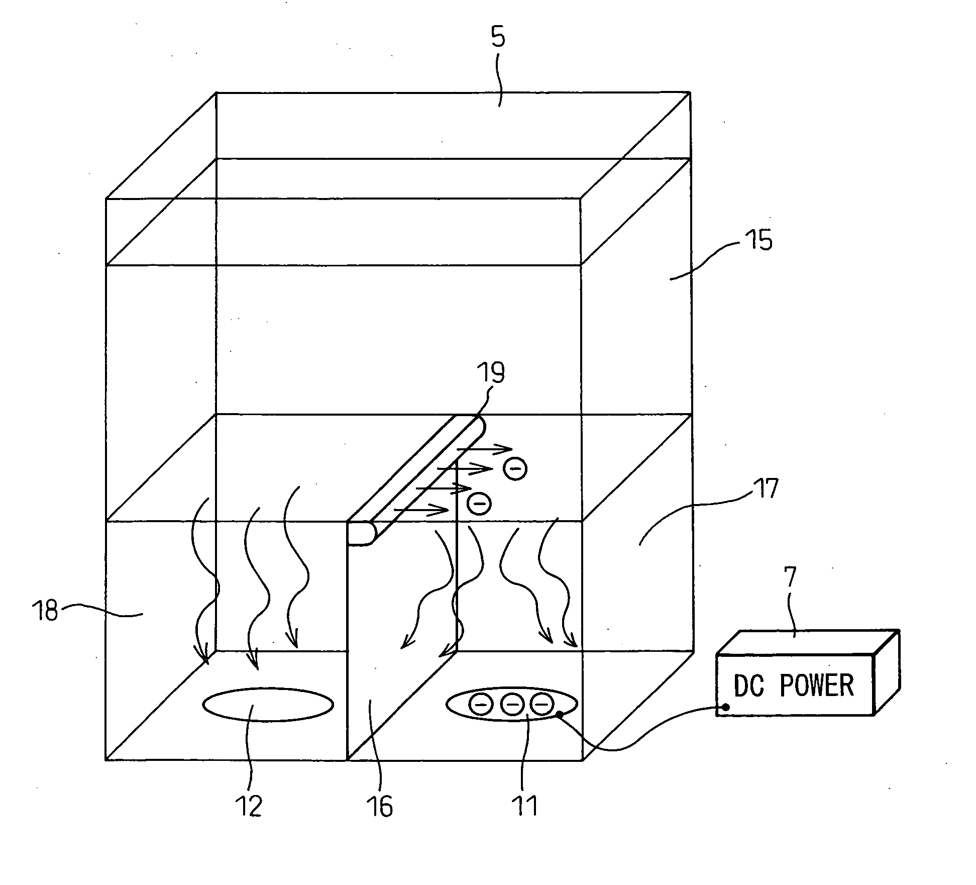
[0119] An example vacuum transfer unit 30 that is provided at a latter stage of a load lock module, for example, shown in FIG. 9 is explained next. The vacuum transfer unit 30 has the gate valves 4, and the carrying arm 2 that carries the semiconductor substrate 1, like the atmospheric transfer unit 10. Further, the vacuum transfer unit 30 has a gas introduction opening 9. Because no air is present in the unit 30, an ionizer using a corona discharge or the like utilizing a discharging between electrodes cannot be used. However, an ultraviolet light generator 8 can be installed in the unit 30 to irradiate ultraviolet rays onto particles within the unit 30, thereby positively charging the particles according to photoelectron emission. Because no ozone is generated in a vacuum, short-wavelength ultraviolet rays can be used at high power. A higher charge effect can be obtained than in the atmosphere.

[0120] An ion generator, an ionization radiation generator, a...

third embodiment

[0122] [Third Embodiment]

[0123] According to the first and the second embodiments, pollution preventing methods of the present invention are applied to the semiconductor substrate transfer unit. However, the pollution preventing methods can be also applied to a processing unit, a load lock module, a semiconductor substrate storing unit, and a semiconductor inspecting unit. A particle charging method suitable for each unit is selected according to the environment (such as vacuum, atmosphere, or inert gas) of the unit to which the invention is applied. A voltage of the same polarity as that of the particle charge is applied to the semiconductor substrate. The charger can be installed at a suitable place, in a similar manner to that according to the first and the second embodiments.

[0124] The semiconductor inspecting unit inspects particles on the substrate, and therefore, it is necessary to strictly manage generation of particles within the unit. From this viewpoint, application of t...


PUM

PropertyMeasurementUnit
Poweraaaaaaaaaa
Sizeaaaaaaaaaa
Electric potential / voltageaaaaaaaaaa

Abstract

In order to prevent particles within a unit from sticking to a substrate in a substrate processing process, an ion generator charges the particles. At the same time, a direct current voltage of the same polarity as the charged polarity of the particles is applied from a direct current power source to the substrate. In order to prevent generation of particles when producing gas plasma, a high-frequency voltage is applied to the upper and lower electrodes at multiple stages to produce plasma. In other words, at a first step, a minimum high-frequency voltage at which plasma can be ignited is applied to the upper and lower electrodes, thereby producing a minimum plasma. Thereafter, the applied voltage is increased in stages to produce predetermined plasma.

Description

BACKGROUND OF THE INVENTION [0001] 1. Field of the Invention [0002] The present invention relates to a device that prevents sticking of particles and restricts generation of particles. Particularly, the invention relates to a particle sticking prevention apparatus and a plasma processing apparatus that restricts generation of particles and prevents sticking of particles in a manufacturing process of semiconductors and flat display panels, for example. [0003] 2. Description of the Related Art [0004] An environment in which manufacturing apparatuses of semiconductors or liquid crystal display units are installed has hardly any problem in cleanliness due to the advanced cleaning of clean rooms. On the other hand, particles that are generated within the manufacturing apparatuses have become a problem. In other words, it is required to prevent the sticking and generation of particles in the manufacturing process. [0005] According to a conventional module that carries a substrate of a sem...

Claims


Application Information

Patent Timeline
IPC IPC(8): B65G49/06C23C16/00H01L21/00H01L21/30H01L21/68
CPCH01J2237/0048H01L21/67069H01L21/67028B01D61/00
Inventor MORIYA, TSUYOSHINAGAIKE, HIROSHIHAYASHI, TERUYUKIFUJIHARA, KAORU
Owner TOKYO ELECTRON LTD
Why Eureka
Try Eureka