Organic light emitting diode

a light-emitting diode and organic technology, applied in the direction of discharge tube/lamp details, organic semiconductor devices, discharge tubes luminescnet screens, etc., can solve the problems of difficult control of sputtering ito or other transparent metal oxide conductors on the organic layer, limited emission area, and easy damage to the layer, etc., to achieve better manufacturing processes, high optical transmission, and high refraction index

Active Publication Date: 2005-04-28
HANNSTAR DISPLAY CORPORATION +1
View PDF17 Cites 46 Cited by
  • Summary
  • Abstract
  • Description
  • Claims
  • Application Information

AI Technical Summary

Benefits of technology

[0014] It is an object of the present invention to provide an organic light emitting diode (OLED). The principal part of the transparent cathode is the transparent dielectric layer with the relatively higher refraction index collocating with the thin metal layer. The transparent cathode of the OLED of the present invention has better manufacturing processes, compliance and relatively higher optical transmission.

Problems solved by technology

Therefore, the emitting area is limited due to the covering by the driver circuit on the substrate.
Because the deposited organic layer is easily damaged during the sputtering process, sputtering ITO or other transparent metal oxide conductors on the organic layer is relatively difficult to control.
However, the major problem of using the thin metal layer as the translucent cathode is that the light transmission is lower.
However, the major problem of such cathode is that the utilized metal has high activity and reactivity such as Ca, Mg, Sr or Li, that is disadvantageous for the environmental stabilization of the components.
The problems of the conventional technology include that the utilized metal belongs to unstable metal with high activity, or the transparent dielectric with high refractive-index value could not be deposited by thermal evaporation.
Moreover, no matter what conductive material is used for the anode of the OLED, usually there is a problem with the hole injection.
Because the difference between the work function of the conductive material and the ionization potential (IP) of the organic opto-electronic materials is disadvantageous for the hole injecting from the anode to the organic layer.

Method used


Image

  • Organic light emitting diode
  • Organic light emitting diode
  • Organic light emitting diode

Examples


Embodiment Construction

[0033] The present invention will now be described more specifically with reference to the following embodiments. It is to be noted that the following descriptions of preferred embodiments of this invention are presented herein for purpose of illustration and description only; it is not intended to be exhaustive or to be limited to the precise form disclosed.

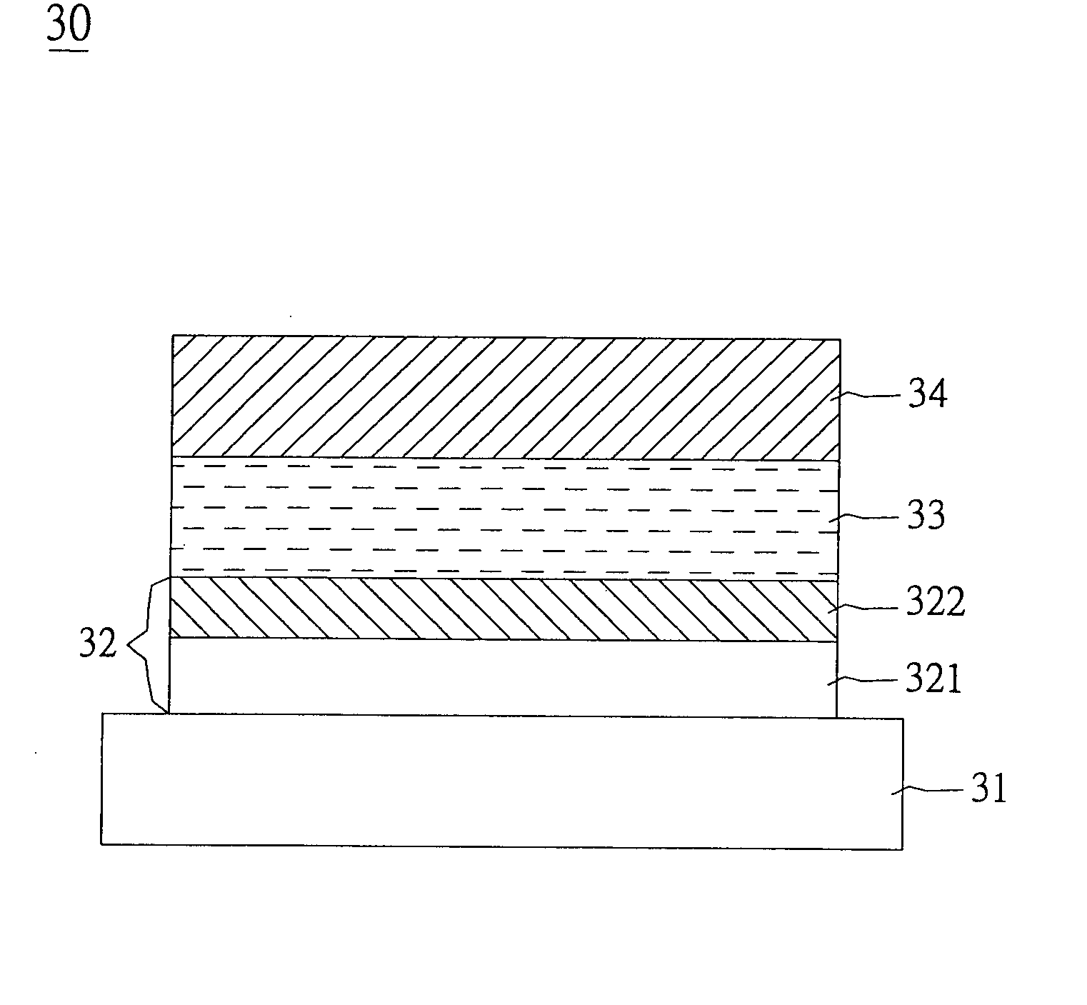
[0034] Please refer to FIG. 3, which is a diagram showing the OLED having the transparent cathode according to a preferred embodiment of the present invention. The OLED includes the substrate 31, the anode 32, the organic layer 33 and the transparent cathode 34. The anode 32 is deposited on the substrate 31. The organic layer 33 is deposited on the anode 32. The transparent cathode 34 is deposited on the organic layer 33. The anode 32 is made of the metal layer 321 and the metal oxide, e.g. AgOx, layer 322 having a thickness ranged between 0.1 and 50 nm deposited on the metal layer 321. Take Ag2O for example, because the Ag2O h...


PUM


Abstract

An organic light emitting diode is provided. The organic light emitting diode includes a substrate, an electrode structure formed on said substrate, an organic layer formed on said electrode structure and a transparent electrode structure having at least one transparent dielectric layer with a relatively higher refraction index and deposited on said organic layer by thermal evaporation.

Description

FIELD OF THE INVENTION [0001] The present invention relates to an organic light emitting diode, and more particularly to an electrode structure of an organic light emitting diode. BACKGROUND OF THE INVENTION [0002] Generally, the organic light emitting diode (OLED) is formed by depositing the organic thin films between the upper metal cathode and the bottom transparent anode. The OLED is manufactured on the transparent substrate, e.g. the glass, and the transparent anode is made of the transparent conductor such as the indium tin oxide (ITO). Please refer to FIG. 1, which is a typical organic light emitting diode with multiple heterogeneous structures. The organic light emitting diode comprises the anode 11, the cathode 17 and a plurality of organic layers with the hole injection layer 12, the hole transport layer 13, the emitting layer 14, the electron transport layer 15, and the electron injection layer 16. Such conventional organic light emitting diode belongs to the bottom-emitt...

Claims


Application Information

Patent Timeline
Patent Type & Authority Applications(United States)
IPC IPC(8): H01J1/62H01J63/04H05B33/26H01L51/00H01L51/30H01L51/50H01L51/52H05B33/14H05B33/22
CPCH01L51/0059H01L51/0081H01L51/5088H01L2251/5315H01L51/5206H01L51/5221H01L51/5092H10K85/631H10K85/324H10K50/17H10K50/171H10K50/818H10K50/82H10K2102/3026
Inventor CHENG, JIA-SHYONGWU, CHUNG-CHIHHSIEH, PING-YUANCHIANG, HUO-HSIENCHEN, CHIEH-WEI
Owner HANNSTAR DISPLAY CORPORATION
Why Eureka
Try Eureka