Epitaxial silicon wafer with intrinsic gettering and a method for the preparation thereof

a silicon wafer and intrinsic gettering technology, applied in the field of silicon wafers and single crystal silicon wafers, can solve the problems of large number of defects in single crystal silicon form in the crystal growth chamber, severely affecting the yield potential of material in the production of complex and highly integrated circuits, and presence of crystal origin pits

Inactive Publication Date: 2005-05-12
SUNEDISON SEMICON LIMITED UEN201334164H
View PDF31 Cites 24 Cited by
  • Summary
  • Abstract
  • Description
  • Claims
  • Application Information

AI Technical Summary

Benefits of technology

[0024] In a further embodiment directed to a process for the preparation of a silicon wafer comprising a surface having an epitaxial layer deposited thereon, the process comprises first heating a wafer comprising a surface with an epitaxial layer deposited thereon to a soak temperature of at least about 1175° C. while exposing the epitaxial layer to an oxidizing atmosphere comprising an oxidant. The heated wafer is then cooled at a rate of at least about 10° C. / sec. In this embodiment, the epitaxial layer has a thickness of at least about 0.1 μm and less than 2.0 μm.
[0025] In another embodiment directed to a process for the preparation of a silicon wafer comprising a surface having an epitaxial layer deposited thereon, the process comprises first depositing an epitaxial layer onto a surface of a wafer starting material to form an epitaxial wafer. The epitaxial wafer is heated to a soak temperature of at least about 1175° C. while exposing the epitaxial layer to an oxidizing atmosphere comprising an oxidant. Afterwards, the heated epitaxial wafer is cooled at a rate of at least about 10° C. / sec. In this embodiment, the surface of the wafer starting material (before the epitaxial layer is deposited onto the surface) has an average light scattering event concentration of at least about 0.5 / cm2 as measured by a laser-based auto inspection tool configured to detect light scattering events corresponding to polystyrene spheres having diameters of no less than about 0.12 μm.

Problems solved by technology

A number of defects in single crystal silicon form in the crystal growth chamber as the crystal cools after solidification.
While these values are relatively low, agglomerated intrinsic point defects are of rapidly increasing importance to device manufacturers and, in fact, are now seen as yield-limiting factors in device fabrication processes and can severely impact the yield potential of the material in the production of complex and highly integrated circuits.
One particularly problematic type of defect is the presence of crystal originated pits (“COPs”).
The source of this type of defect is the agglomeration of silicon lattice vacancies.
More specifically, when silicon lattice vacancies agglomerate within a silicon ingot, they form voids.
While this approach reduces the number density of agglomerated defects, it does not prevent their formation.
As the requirements imposed by device manufacturers become more and more stringent, the presence of these defects will continue to become more of a problem.
This suggestion, however, is also not satisfactory because such a slow pull rate leads to reduced throughput for each crystal puller.
This high concentration, in turn, leads to the formation of agglomerated self-interstitial defects and all the resulting problems associated with such defects.
Further, such wafer heat treatments are relatively costly, have the potential for introducing metallic impurities into the silicon wafers, and are not universally effective for all types of crystal-related defects.
Use of the traditional epitaxial deposition techniques, however, substantially increases the cost of the wafer.
This contamination, for example, occurs while the molten silicon is contained in the quartz crucible.
Depending on their location in the wafer, the precipitates can be harmful or beneficial.
Oxygen precipitates located in the active device region of the wafer (i.e., typically near the surface) can impair the operation of the device.
Although some of these processes retain enough of the high temperature process steps to produce a denuded zone and sufficient density of bulk precipitates, the tolerances on the material are too tight to render it a commercially viable product.
Because of the problems associated with oxygen precipitates in the active device region, therefore, these electronic device fabricators must use silicon wafers which are incapable of forming oxygen precipitates anywhere in the wafer under their process conditions.
As a result, IG potential is lost.

Method used


Image

  • Epitaxial silicon wafer with intrinsic gettering and a method for the preparation thereof
  • Epitaxial silicon wafer with intrinsic gettering and a method for the preparation thereof
  • Epitaxial silicon wafer with intrinsic gettering and a method for the preparation thereof

Examples


Embodiment Construction

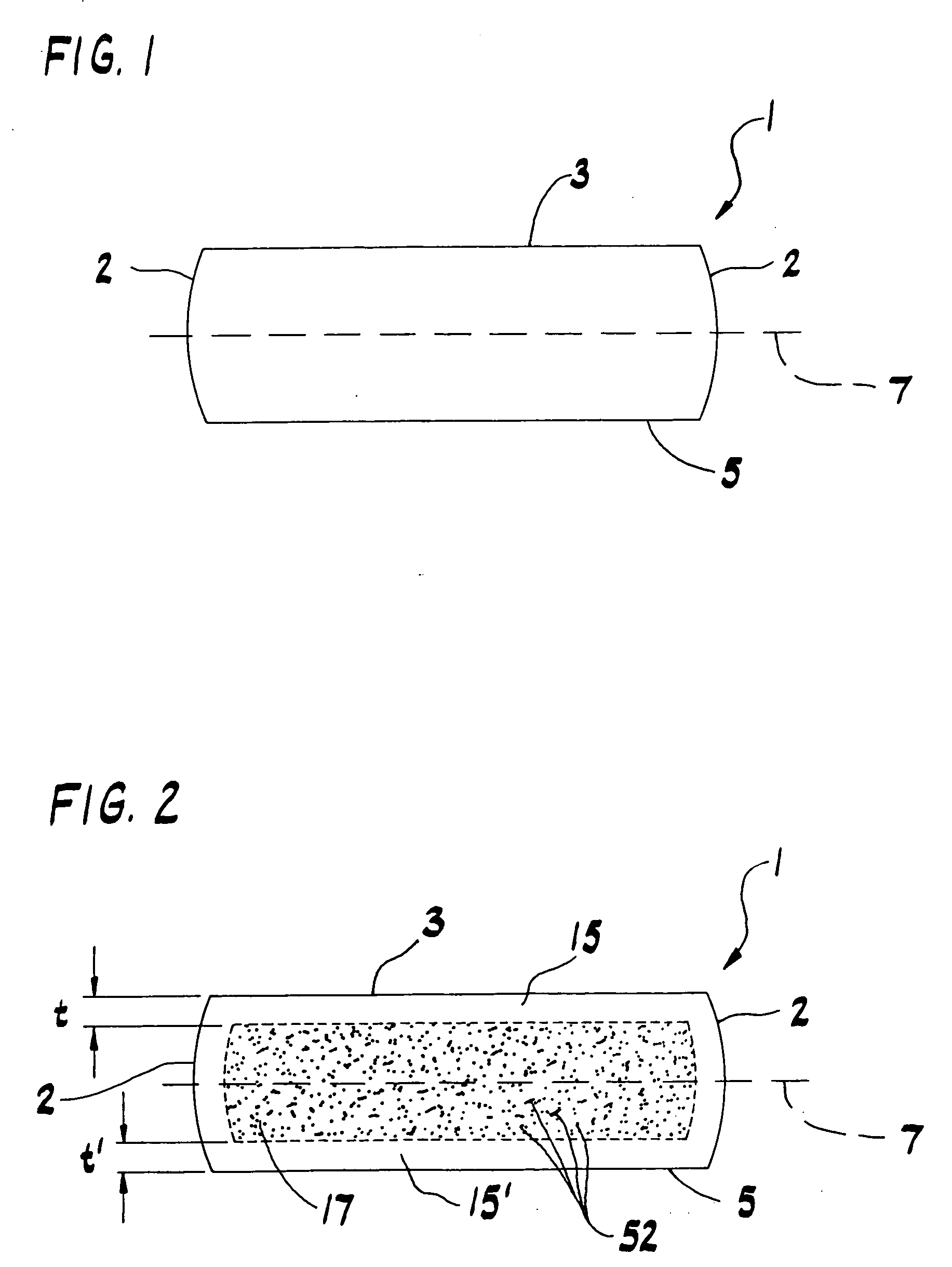
[0037] In accordance with the present invention, a novel and useful single crystal silicon wafer comprising a surface having an epitaxial silicon layer deposited thereon has been developed. The epitaxial surface of the wafer typically has an average light scattering event concentration of no greater than about 0.06 / cm2, as measured by a laser-based auto inspection tool configured to detect light scattering events corresponding to polystyrene spheres having diameters of no less than about 0.12 μm. In addition, the wafer contains a “template” that determines (or “prints”) the manner in which oxygen will precipitate when the wafer is heated during the electronic device manufacturing process. Thus, during a heating step of essentially any electronic device manufacturing process, the wafer will form (a) a denuded zone of sufficient depth, and (b) a wafer bulk containing a sufficient density of oxygen precipitates for IG purposes. Also in accordance with this invention, a novel method has...


PUM

PropertyMeasurementUnit
distanceaaaaaaaaaa
thicknessaaaaaaaaaa
distanceaaaaaaaaaa

Abstract

A wafer is characterized in that the wafer has a non-uniform distribution of crystal lattice vacancies, wherein the concentration of crystal lattice vacancies in the bulk layer are greater than the concentration of crystal lattice vacancies in the front surface layer. In addition, the front surface of the wafer has an epitaxial layer, having a thickness of less than about 2.0 μm, deposited thereon. A process comprises heating a surface of a wafer starting material to remove a silicon oxide layer from the surface and depositing an epitaxial layer onto the surface to form an epitaxial wafer. The epitaxial wafer is then heated to a soak temperature of at least about 1175° C. while exposing the epitaxial layer to an oxidizing atmosphere comprising an oxidant, and the wafer is cooled at a rate of at least about 10° C./sec.

Description

CROSS-REFERENCE TO RELATED APPLICATION [0001] This is a division of application Ser. No. 09 / 859,094, filed May 16, 2001, now U.S. Pat. No. 6,537,655, which is a division of application Ser. No. 09 / 250,908, filed Feb. 16, 1999, now U.S. Pat. No. 6,284,384, which claims the benefit of U.S. Provisional Application No. 60 / 111,546, filed Dec. 9, 1998.BACKGROUND OF THE INVENTION [0002] The present invention generally relates to the preparation of semiconductor material substrates, especially silicon wafers, which are used in the manufacture of electronic components. More particularly, the present invention relates to a single crystal silicon wafer and a method for the preparation thereof. This wafer comprises a surface having an epitaxial silicon layer deposited thereon, and forms an ideal, non-uniform depth distribution of oxygen precipitates during the heat treatment cycles of essentially any electronic device manufacturing process. [0003] Single crystal silicon, which is the starting m...

Claims


Application Information

Patent Timeline
Patent Type & Authority Applications(United States)
IPC IPC(8): C30B25/10C30B33/00H01L21/322H01L21/205
CPCC30B25/10C30B29/06Y10S257/913H01L21/3225C30B33/00Y10T428/249961Y10T428/249978H01L21/20
Inventor WILSON, GREGORY M.ROSSI, JON A.YANG, CHARLES C.
Owner SUNEDISON SEMICON LIMITED UEN201334164H
Why Eureka
Try Eureka