Vicinal gallium nitride substrate for high quality homoepitaxy

a technology of vicinal gallium nitride and homoepitaxy, which is applied in the direction of natural mineral layered products, polycrystalline material growth, transportation and packaging, etc., can solve the problems of adversely affecting device performance, and achieve the effect of high quality

Active Publication Date: 2005-05-19
WOLFSPEED INC
View PDF6 Cites 61 Cited by
  • Summary
  • Abstract
  • Description
  • Claims
  • Application Information

AI Technical Summary

Benefits of technology

[0011] The present invention relates to vicinal III-V nitride substrates, e.g., gallium nitride substrates, having suitability for high quality homoepitaxial fabrication of microelectronic and opto-electronic device structures.

Problems solved by technology

Due to the resultant mismatch of lattice constants and thermal coefficient of expansion differences between the gallium nitride device layers and the foreign substrate, a high density of defects typically is produced in the gallium nitride device layers, adversely affecting device performance.

Method used


Image

  • Vicinal gallium nitride substrate for high quality homoepitaxy
  • Vicinal gallium nitride substrate for high quality homoepitaxy
  • Vicinal gallium nitride substrate for high quality homoepitaxy

Examples


example 1

[0084] A vicinal GaN substrate with 1 degree offcut towards −10> direction was used as a substrate for homoepitaxial growth.

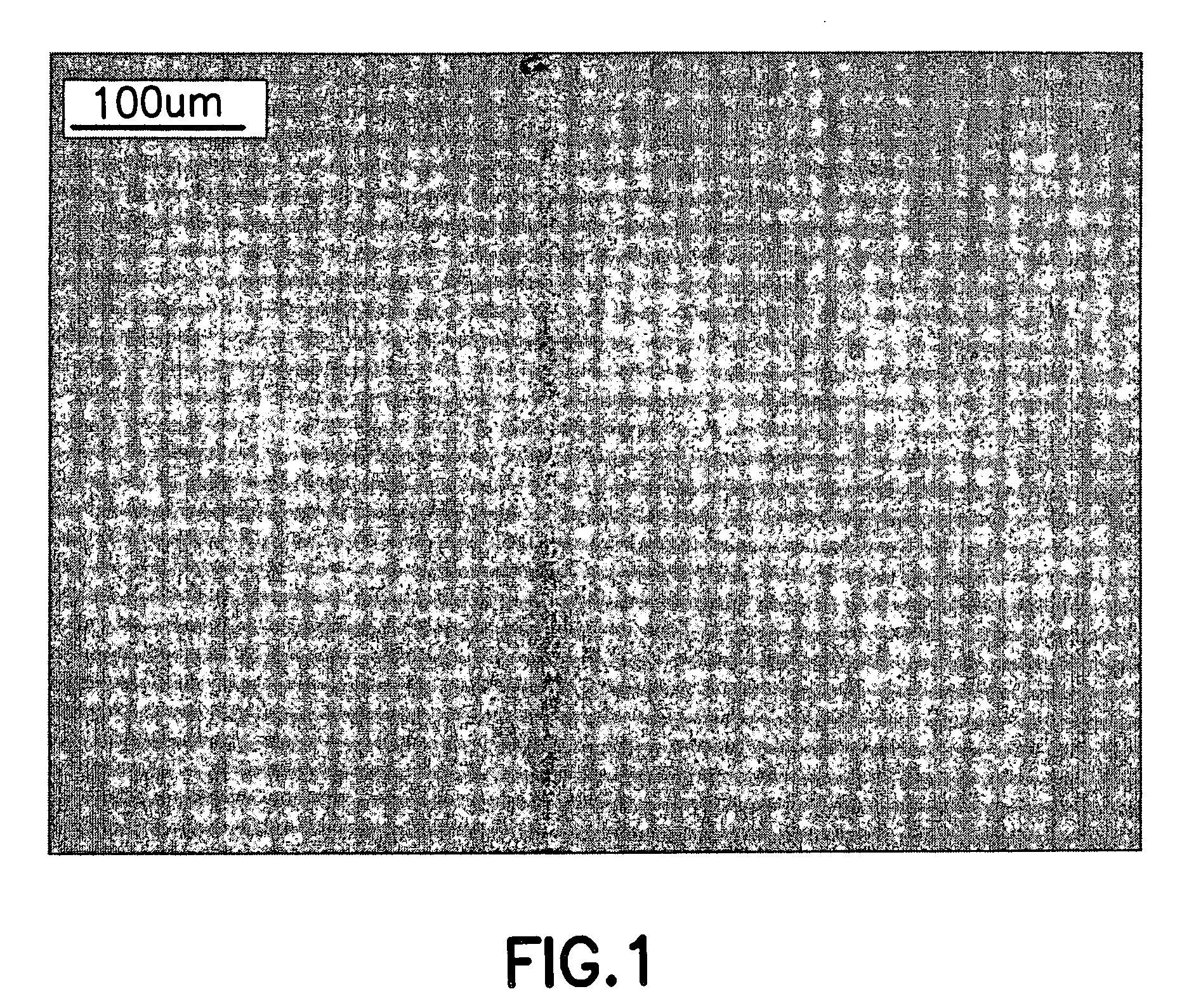
[0085]FIG. 12 is a DIC microscope image of the wafer surface near the center and near the edge for a 2-μm homoepitaxial film grown on such vicinal GaN substrate (1 degree towards ) under the following growth conditions: growth rate=2 μm / hr and growth temperature=1120° C. The homoepitaxial film was uniformly smooth, in contrast to a nominally c-plane substrate on which a non-uniform homoepitaxial film was grown.

[0086] Under the DIC optical microscope, the homoepitaxial GaN film on the vicinal GaN wafer was smooth and featureless over the entire wafer surface, as shown in FIG. 12. Optical surface morphology of the GaN film near the edge of the vicinal substrate was identical to the morphology of the GaN film near the center of the vicinal substrate.

[0087] AFM was further utilized to characterize surface microstructure of the GaN film on the vicinal GaN substra...

example 2

[0089] An AlGaN / GaN high electron mobility transistor (HEMT) structure was grown on a vicinal GaN (0001) substrate (2 degree offcut towards the direction) under the following growth conditions: growth rate=2 μm / hr and growth temperature=1170° C. The HEMT structure consisted of a 2 μm thick undoped MOVPE homoepitaxial GaN film on the vicinal substrate and 25 nm AlGaN (30 atomic % Al) layer on top of the homoepitaxial GaN film. The HEMT wafer had uniform and smooth surface morphology when examined under an optical microscope. The hillock morphology typically observed on the homoepitaxial surface on a c-plane GaN (0001) substrate was absent on the vicinal GaN wafer.

[0090]FIG. 15 is a 2×2 μm2 AFM scan of the HEMT structure grown on the 2 degree offcut (towards ) GaN (0001) substrate, showing a smooth surface morphology with step structures.

[0091]FIG. 16 is a capacitance-voltage (CV) measurement of the HEMT structure with a mercury probe, confirming that a two-dimensional electron gas...

example 3

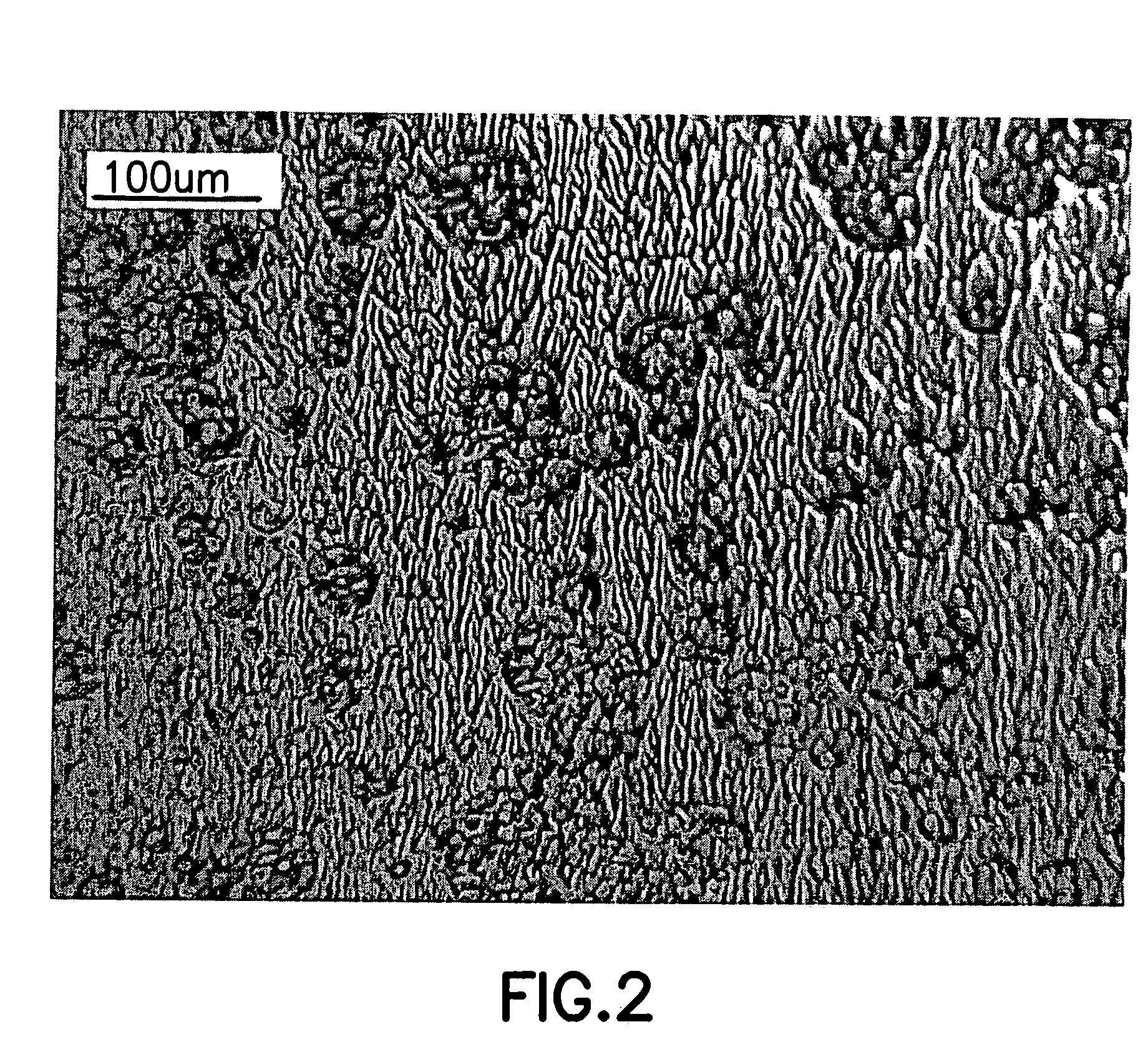
[0092] An AlGaN / GaN high electron mobility transistor (HEMT) structure was grown on an 8 degree offcut (towards direction) GaN (0001) substrate under the following growth conditions: growth rate=2 μm / hr and growth temperature=1170° C. The HEMT structure consisted of a thick 2 μm undoped MOVPE homoepitaxial GaN film on the vicinal substrate and 25 nm AlGaN (30 atomic % Al) layer on top of the homoepitaxial GaN film. The surface morphology of the HEMT structure was smooth and replicated the substrate morphology.

[0093]FIG. 17 is a DIC microscope image of the surface of the HEMT structure grown on the 8 degree (towards ) vicinal GaN (0001) substrate, and the HEMT surface replicated the substrate surface. The entire wafer surface was uniform, without any hillock morphology.

[0094]FIG. 18 is a capacitance-voltage measurement of the HEMT device layer grown on the 8 degree offcut (towards ) GaN (0001) substrate. The sharp pinch-off demonstrated a good 2DEG in the AlGaN / GaN interface regio...


PUM

PropertyMeasurementUnit
dislocation densityaaaaaaaaaa
RMS roughnessaaaaaaaaaa
offcut angleaaaaaaaaaa

Abstract

A III-V nitride, e.g., GaN, substrate including a (0001) surface offcut from the <0001> direction predominantly toward a direction selected from the group consisting of <10-10> and <11-20> directions, at an offcut angle in a range that is from about 0.2 to about 10 degrees, wherein the surface has a RMS roughness measured by 50×50 μm2 AFM scan that is less than 1 nm, and a dislocation density that is less than 3E6 cm−2. The substrate may be formed by offcut slicing of a corresponding boule or wafer blank, by offcut lapping or growth of the substrate body on a corresponding vicinal heteroepitaxial substrate, e.g., of offcut sapphire. The substrate is usefully employed for homoepitaxial deposition in the fabrication of III-V nitride-based microelectronic and opto-electronic devices.

Description

BACKGROUND OF THE INVENTION [0001] 1. Field of the Invention [0002] The present invention relates to vicinal III-V nitride substrates, e.g., vicinal gallium nitride substrates, such as are usefully employed for deposit of homoepitaxial films thereon in the fabrication of high quality electronic and opto-electronic devices. [0003] 2. Description of the Related Art [0004] Gallium nitride (GaN) and related III-IV nitride alloys are wide bandgap semiconductor materials that have application in opto-electronics (e.g., in fabrication of blue and UV light emitting diodes and laser diodes) and in high-frequency, high-temperature and high-power electronics. In such high-performance devices, high quality epitaxial films must be grown on the substrate. [0005] Gallium nitride-based electronic devices are typically grown on foreign (heteroepitaxial) substrates such as sapphire and silicon carbide. Due to the resultant mismatch of lattice constants and thermal coefficient of expansion differences...

Claims


Application Information

Patent Timeline
Patent Type & Authority Applications(United States)
IPC IPC(8): H01L29/04H01L29/20
CPCC30B25/18C30B29/403Y10T428/31H01L29/045H01L29/2003C30B29/406Y10T83/0524H01L21/20
Inventor XU, XUEPINGVAUDO, ROBERT P.FLYNN, JEFFREY S.BRANDES, GEORGE R.
Owner WOLFSPEED INC
Why Eureka
Try Eureka