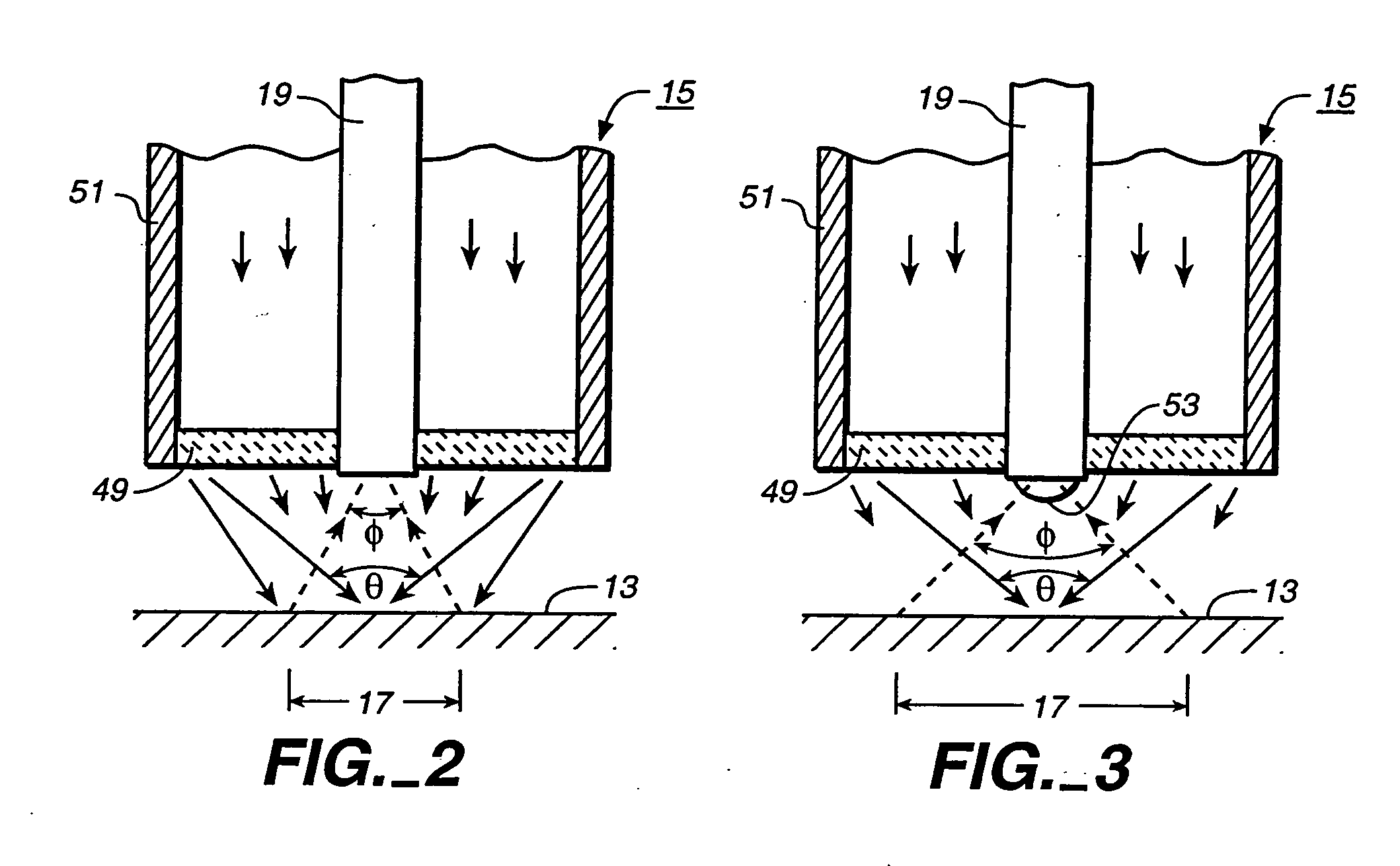
[0011] The wide angle illumination and detection significantly reduces the effects of variations in scattering of the optical signals that can occur independently of the quantity desired to be measured. The incident
optical radiation, and that modified by the surface being monitored, can be scattered varying amounts that depend upon the surface, angles that the radiation strikes the surface and optical elements, changes over time, and other causes. If the viewing angle is too narrow for a given angular extent of the illumination, for example, any variation in the amount of incident radiation that is scatted into the narrow viewing angle because of differences in scattering properties across the surface being monitored or between different surfaces, versus that which is scattered over wider angles out of view, causes the detected optical
signal to vary. Significant variations can also occur when the surface is being viewed through a
liquid layer, such as an etchant or
slurry, that changes its thickness and other characteristics over time. These factors often cause the measurement
signal to have significant amounts of undesired
noise. But if the surface is illuminated and viewed over wide angles relative to that through which the incident radiation is scattered by the surface, any liquid etchant on it and by the optical elements, this source of noise is significantly reduced. It is reduced further when the surface is illuminated over wide angles. Illumination and detection over a full hemisphere is ideal but significant improvements are made when lesser angles in the range given above are utilized.
[0012] If a surface is illuminated with radiation over a very wide angle, such as 80 degrees or more, the
surface modified radiation may be gathered for detection over a small angle, such as 25 or 15 degrees or less, and still provide the advantages described above. A small collection angle is often desired for other purposes, such as to increase the
depth of focus of the collection
optics, allow practical sized collection
optics, increase the sensitivity of the measurement to the thickness of a films being monitored, in those applications, and / or to focus on a very small spot on the surface being monitored.
[0015] When the monitored layer is a
metal or other generally opaque material, its
reflectivity and
emissivity are directly related to the thickness of the layer if the layer is thin enough to be at least partially transparent. For example, when a
metal layer is being removed from a substrate, the layer's reflectivity or emissivity, when measured by the techniques summarized above, is directly related to the thickness of the metal layer once it has become thin enough to be semi-transparent. A metal film on a
semiconductor wafer is semi-transparent when its thickness is less than about 500 to 1500 Angstroms, depending on the metal and the
wavelength of radiation used. Therefore, for such
thin metal layers, their thicknesses can be determined from a look-up table or set of functions that relate the measured reflectivity or emissivity with the layer's thickness. This makes it possible to measure and control the thicknesses of
thin metal films with precision. Once the metal film is completely removed, then the optical properties being measured are those of the
layers under the metal film. The measurement of the reflectivity or emissivity of a metal layer can be conducted with one or more wavelengths of
optical radiation.
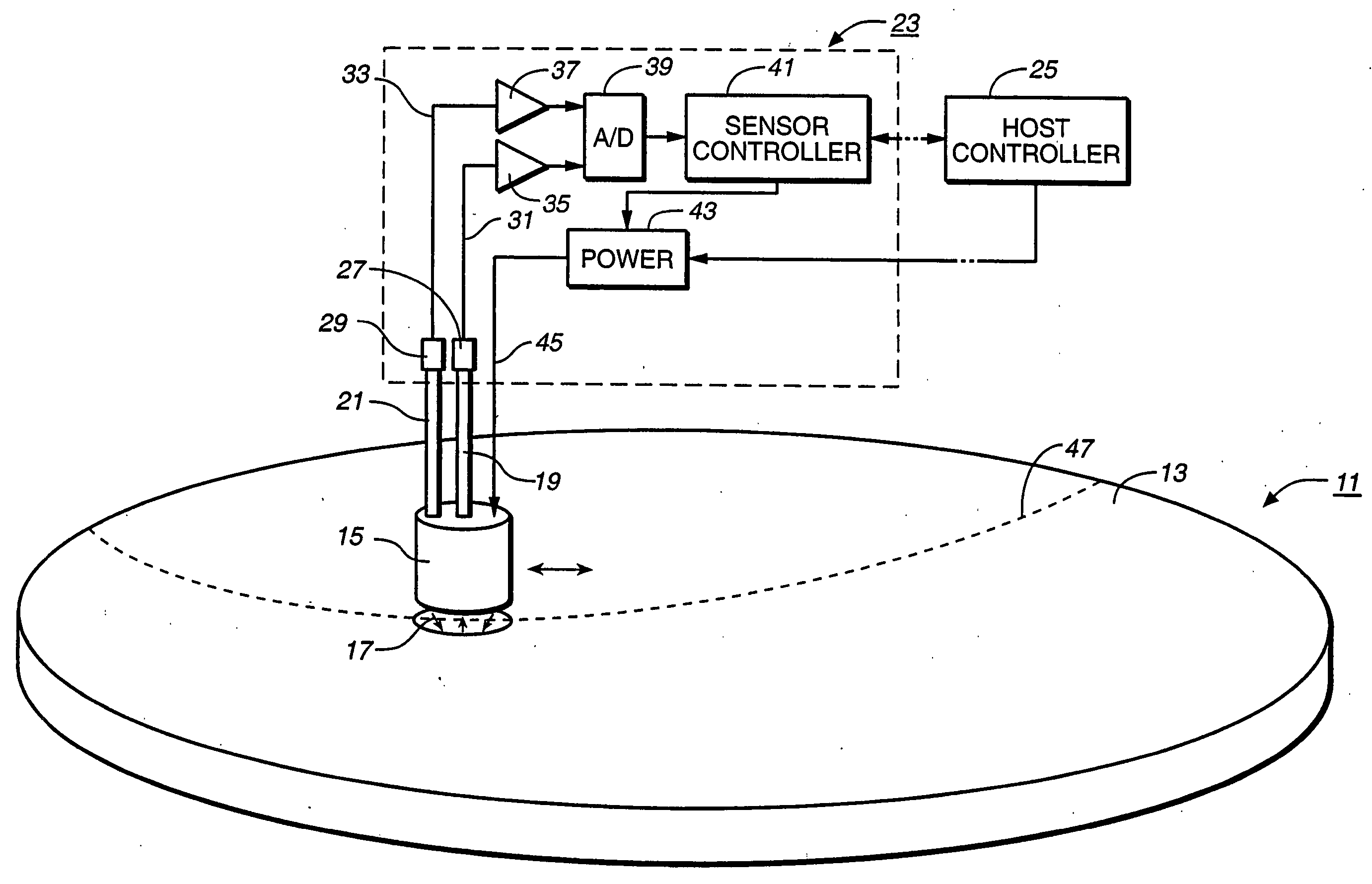
[0017] When two or more wavelengths of radiation are used to illuminate a layer, the radiation can be generated by separate
narrow bandwidth radiation sources, such as light emitting diodes (LEDs), and then the uniquely responsive to one of the source wavelengths. Alternatively, or in combination, the two or more radiation sources are each modulated with a unique frequency. Electrical signals obtained from a single or multiple radiation receiving photodetectors are then filtered to pass the source modulating frequencies in order to obtain a separate signal for each of the illumination wavelengths. The frequencies of modulation are preferably selected to be different from that of any ambient radiation or electrical noise that might be present in the environment in which the measurements are being taken, thereby to significantly reduce adverse effects of any such ambient radiation and noise. The radiation source modulation and
photodetector signal filtering technique can also be used when a single optical radiation is directed at the surface being monitored in order to similarly reduce the effects of any ambient radiation and electrical noise that might be present at different frequencies from the modulating frequency.

