Built in self test circuit for measuring total timing uncertainty in a digital data path

a self-testing, digital data path technology, applied in the direction of pulse characteristics measurement, instruments, horology, etc., can solve the problems of timing uncertainty, latches that randomly enter metastability, latches that cannot be loaded correctly, etc., to achieve accurate recovery of vdd power bus noise waveform

Inactive Publication Date: 2005-05-19
GLOBALFOUNDRIES INC
View PDF24 Cites 40 Cited by
  • Summary
  • Abstract
  • Description
  • Claims
  • Application Information

AI Technical Summary

Benefits of technology

[0013] It is yet another purpose of the invention to accurately determine the number of completed logic stages on a cycle by cycle basis and monitor and log the worst-case timing variations.
[0014] It is yet another purpose of this invention to accurately recover t

Problems solved by technology

Unfortunately, various chip differences can cause timing uncertainty, i.e., a variation in edge arrival to different registers.
Such timing uncertainties can arise from data propagation variations and/or from clock arrival variations.
Data propagation variations, for example, may result in a capturing latch that randomly enters metastability or latches invalid data because the data may or may not arrive at its input with sufficient set up time.
In particular, power supply noise can cause clock propagation delay variations through clock distribution buffers.
Such clock propagation delay variations can cause skew variations from clock edge arrival time uncertainty at the registers.
Especially for clock distribution buffers, these process variations are another source of timing uncertainty.
Furthermore, as technology features continue to shrink, power bus or Vdd noise is becoming the dominant contributor to total timing uncertainty.
High speed circuit switching may cause large, narrow current spikes with very rapid rise and fall times, i.e., large

Method used


Image

  • Built in self test circuit for measuring total timing uncertainty in a digital data path
  • Built in self test circuit for measuring total timing uncertainty in a digital data path
  • Built in self test circuit for measuring total timing uncertainty in a digital data path

Examples


Embodiment Construction

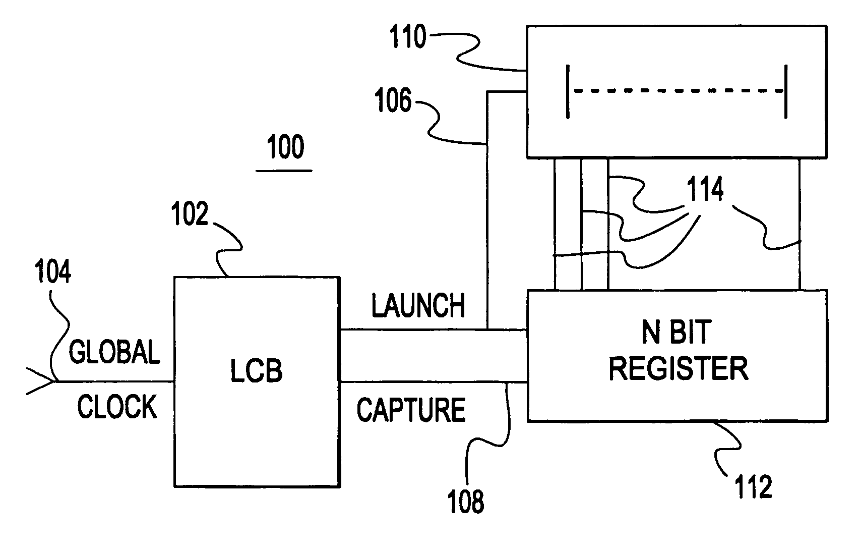
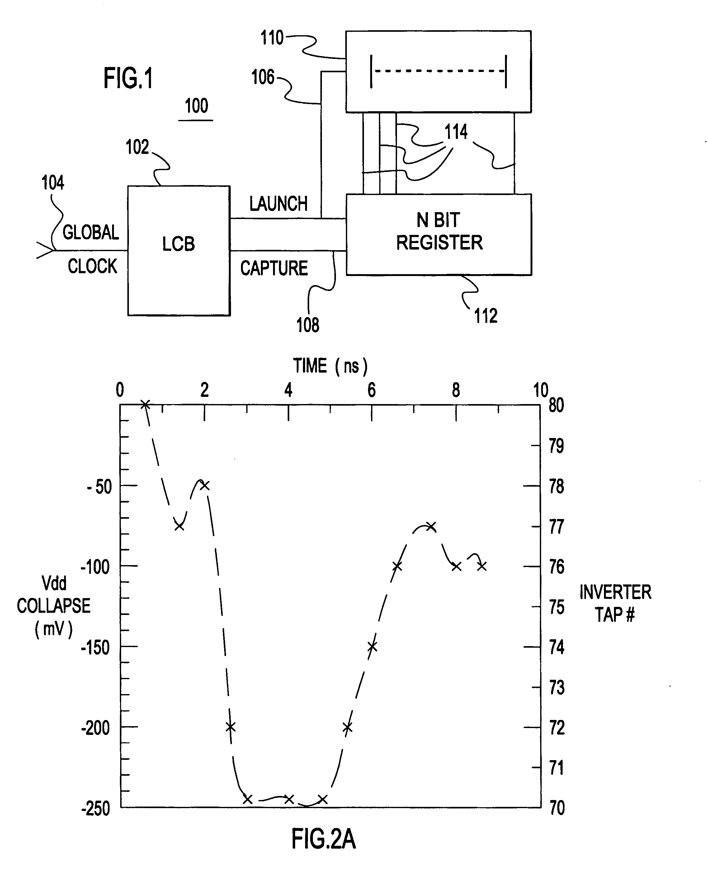
[0026] Turning now to the drawings and, more particularly, FIG. 1 shows a block diagram of an example of a logic stage counter 100 according to a preferred embodiment of the present invention. A local clock block (LCB) or clock buffer 102 receives and re-drives a global chip clock 104 into 2 complementary local clocks 106, 108. One clock, a launch clock 106, is provided to a delay line 110 and launches the timing edge in the delay. The LCB 102 and delay line 110 mimic data propagation delay through an actual data path, e.g., in a microprocessor. Both clocks 106, 108 clock an N bit register 112. Delay line taps 114 are stage inputs to N bit register 112. For example, N=129 may be a convenient length for holding 3 cycles worth of edges. The second clock, a capture clock 108, captures the forward position of the timing edges in the N bit register 112. Although in this example, the launch clock 106 drives the delay line 110, either clock, the launch or the capture clock can drive the de...


PUM


Abstract

A circuit for measuring timing uncertainty in a clocked digital path and in particular, the number of logic stages completed in any clock cycle. A local clock buffer receives a global clock and provides a complementary pair of local clocks. A first local (launch) clock is an input to a delay line, e.g., 3 clock cycles worth of series connected inverters. Delay line taps (inverter outputs) are inputs to a register that is clocked by the complementary clock pair to capture progression of the launch clock through the delay line and identify any variation (e.g., from jitter, VDD noise) in that progression. Global clock skew and across chip gate length variation can be measured by cross coupling launch clocks from a pair of such clock buffers and selectively passing the local and remote launch clocks to the respective delay lines.

Description

CROSS REFERENCE TO RELATED APPLICATION [0001] The present invention is related to U.S. application Ser. No. ______ (Attorney Docket No. YOR20030364US1) entitled “CLOCK GATED POWER SUPPLY NOISE COMPENSATION” to Phillip J. Restle, filed coincident herewith and assigned to the assignee of the present invention.BACKGROUND OF THE INVENTION [0002] 1. Field of the Invention [0003] The present invention is related to integrated circuit (IC) design systems and more particularly to characterizing timing uncertainties in ICs. [0004] 2. Background Description [0005] Large high performance very large scale integration (VLSI) chips like microprocessors are synchronized to an internal clock. A typical internal clock is distributed throughout the chip, triggering chip registers to synchronously capture incoming data at the register latches and launch data from register latches. Ideally, each clock edge arrives simultaneously at each register every cycle and data arrives at the register latches suff...

Claims


Application Information

Patent Timeline
IPC IPC(8): G01R31/317G01R31/3185G06F19/00
CPCG01R31/318594G01R31/31725
Inventor FRANCH, ROBERT L.HUOTT, WILLIAM V.JAMES, NORMAN K.RESTLE, PHILLIP J.SKERGAN, TIMOTHY M.
Owner GLOBALFOUNDRIES INC
Why Eureka
Try Eureka