Method and structure to enhance temperature/humidity/bias performance of semiconductor devices by surface modification

a technology of bias performance and surface modification, which is applied in the direction of semiconductor devices, semiconductor/solid-state device details, electrical devices, etc., can solve the problems of cracks at the terminal insulator level of the chip, and cracks of glass dielectric materials such as sicoh or carbon-doped oxide under applied stress. , to achieve the effect of enhancing the temperature/humidity/

Inactive Publication Date: 2005-06-02
GLOBALFOUNDRIES INC
View PDF13 Cites 13 Cited by
  • Summary
  • Abstract
  • Description
  • Claims
  • Application Information

AI Technical Summary

Benefits of technology

[0012] It is therefore an object the present invention to provide a method for repairing or sealing damage on semiconductor chips due to electrical connections such as wire bonds, and more generally for enhancing temperature / humidity / bias performance of semiconductor chips using a low-cost method which does not introduce unconventional materials or additional metal layers.

Problems solved by technology

Glass dielectric materials such as SiCOH or carbon-doped oxide tend to crack under applied stress and in humid atmosphere, while organic thermoset polymers do not.
However, one disadvantage is the low modulus of organic polymer or low k CVD dielectrics, which can result in defects or breaches formed in the passivation layers when the completed IC chip is electrically connected via wirebonding (or soldering) methods to an IC holder.
Cracks often occur as well at the terminal insulator level of the chip.
These cracks have many causes; most notable are those caused by rough handling of the finished chip prior to packaging and the damage that can result during the die wire bonding process.
Delamination of the passivation layers is also a possible problem.
However, this terminal inorganic oxide is more easily damaged than in devices using oxide for all inter-layer dielectric, due to the unique mechanical structure of low-k dielectric integration.
Furthermore, as device ground rules continue to decrease, even without the transition to low-k dielectrics, these microcracks and delaminations are likely to become a significant source of device performance degradation if they are left unrepaired before final packaging and encapsulation.
Post wire-bond packaging and encapsulation processes are ineffective in sealing these cracks in the terminal insulator level of the chip.
As a result of the lack of seal or repair of these cracks in the terminal insulator level of the chip, electrical degradation in semiconductor chip electrical performance has been observed during temperature and humidity stress testing.
However, it has been observed that such polymers alone can not provide an effective barrier to moisture ingress.
However, the use of unconventional materials and additional metal layers adds significantly to the cost of the manufacturing process.

Method used


Image

  • Method and structure to enhance temperature/humidity/bias performance of semiconductor devices by surface modification
  • Method and structure to enhance temperature/humidity/bias performance of semiconductor devices by surface modification
  • Method and structure to enhance temperature/humidity/bias performance of semiconductor devices by surface modification

Examples


Embodiment Construction

[0019] The invention will now be described by reference to the accompanying figures. In the figures, various aspects of the structures have been shown and schematically represented in a simplified manner to more clearly describe and illustrate the invention. For example, the figures are not intended to be to scale. In addition, the vertical cross-sections of the various aspects of the structures are illustrated as being rectangular in shape. Those skilled in the art will appreciate, however, that with practical structures these aspects will most likely incorporate more tapered features. Moreover, the invention is not limited to constructions of any particular shape.

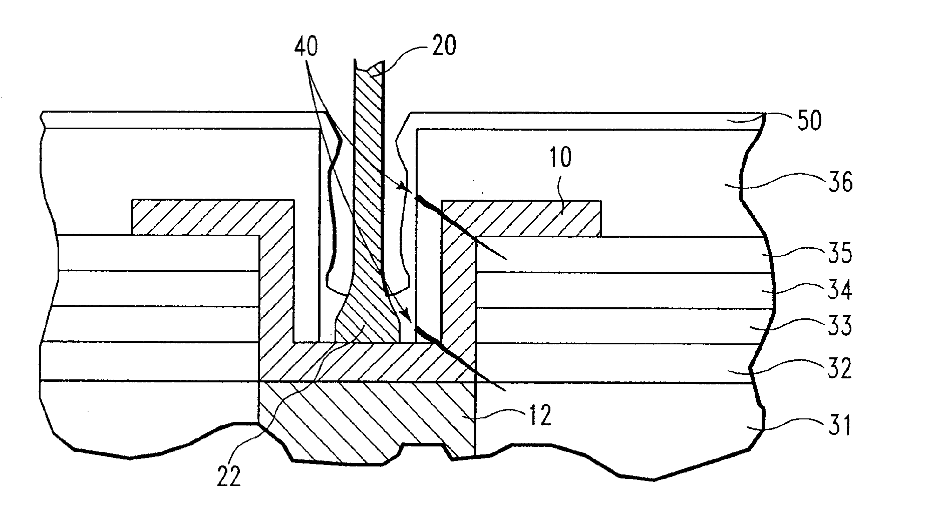
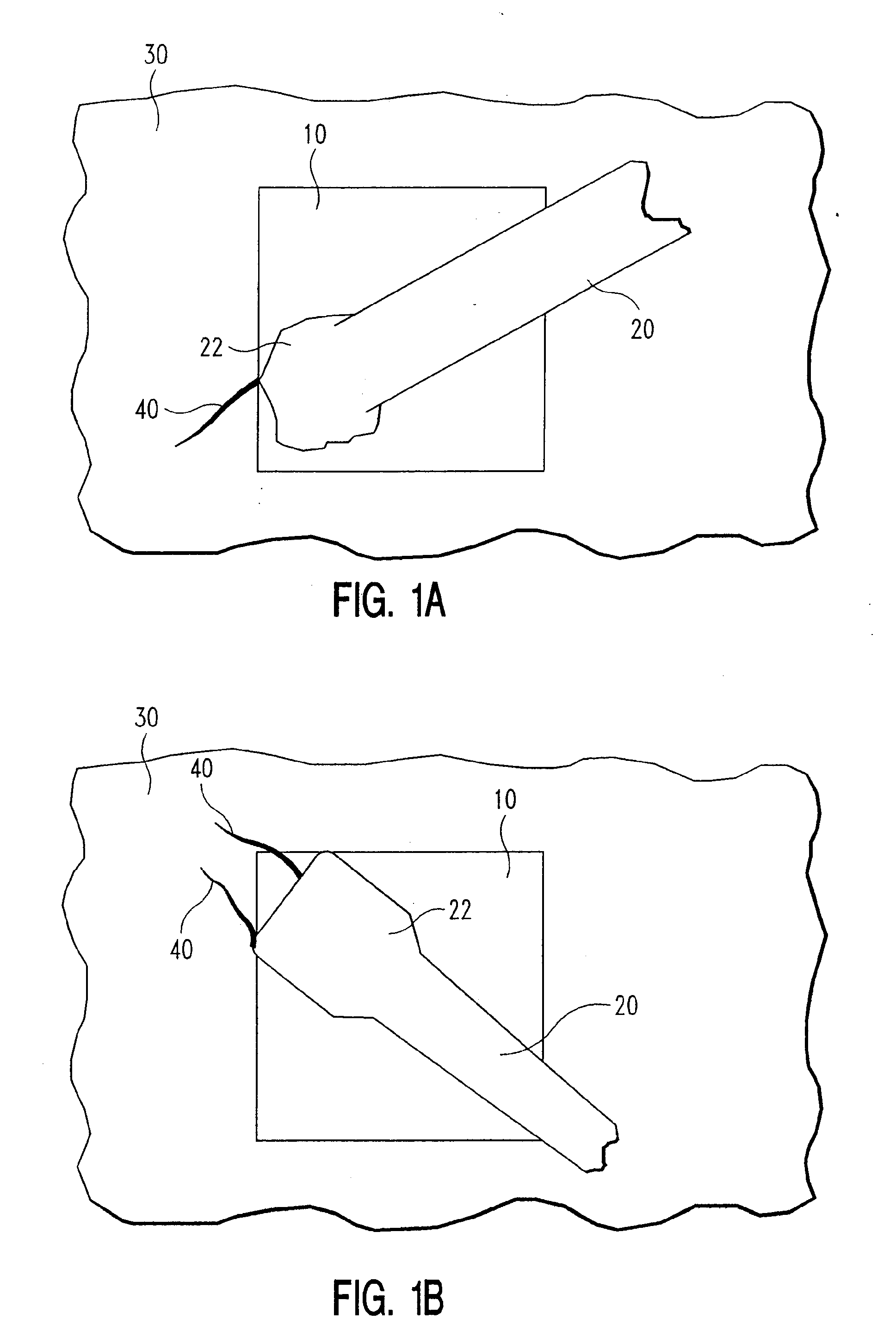
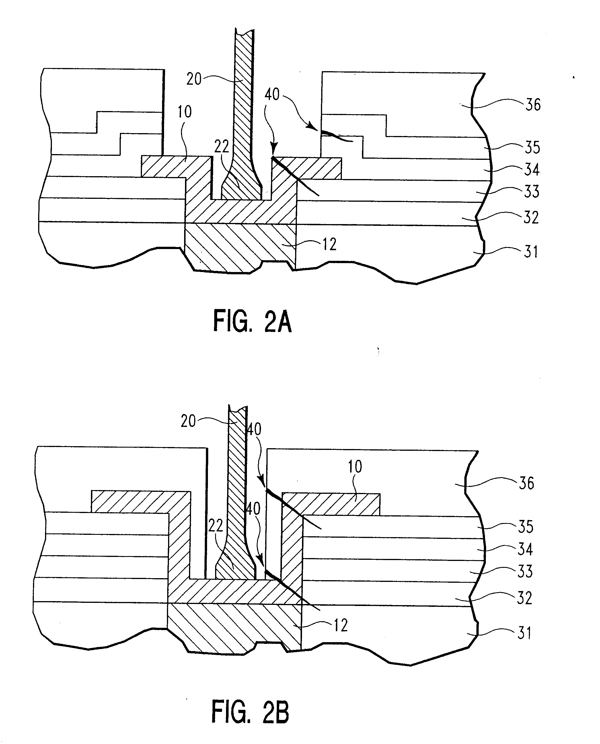
[0020] In one aspect, this invention is a method to repair and seal microcracks and delaminations that are found in typical damage due to wire bonds or other electrical connections. A damaged part may be, for example, an integrated circuit chip mounted on a chip carrier or interposer, in which the chip contains damage wh...


PUM


Abstract

A method is disclosed of repairing wirebond damage on semiconductor chips such as high speed semiconductor microprocessors, application specific integrated circuits (ASICs), and other high speed integrated circuit devices, particularly devices using low-k dielectric materials. The method involves surface modification using reactive liquids. In a preferred embodiment, the method comprises applying a silicon-containing liquid reagent precursor such as TEOS to the surface of the chip and allowing the liquid reagent to react with moisture to form a solid dielectric plug or film (50) to produce a barrier against moisture ingress, thereby enhancing the temperature/humidity/bias (THB) performance of such semiconductor devices.

Description

TECHNICAL FIELD [0001] This invention relates generally to the manufacture of high speed semiconductor microprocessors, application specific integrated circuits (ASICs), and other high speed integrated circuit devices. More particularly, this invention relates to a method to enhance the temperature / humidity / bias (THB) performance of such semiconductor devices, particularly devices using low-k dielectric materials, by surface modification using reactive liquids. BACKGROUND OF THE INVENTION [0002] Metal interconnections in very large scale integrated (VLSI) or ultra-large scale integrated (ULSI) circuits typically consist of interconnect structures containing patterned layers of metal wiring. Typical integrated circuit (IC) devices contain from three to fifteen layers of metal wiring. As feature size decreases and device area density increases, the number of interconnect layers is expected to increase. [0003] The materials and layout of these interconnect structures are preferably cho...

Claims


Application Information

Patent Timeline
Patent Type & Authority Applications(United States)
IPC IPC(8): H01L21/44H01L21/4763H01L21/48H01L21/50H01L23/00H01L23/28
CPCH01L23/564H01L24/05H01L2224/04042H01L2924/01074H01L2924/01033H01L2924/01019H01L24/48H01L2924/1433H01L2924/14H01L2224/05009H01L2224/05556H01L2224/05624H01L2224/48463H01L2924/01005H01L2924/01006H01L2924/01013H01L2924/01014H01L2924/01029H01L2924/01079H01L2924/014H01L2924/00014H01L2924/00H01L2224/02166H01L2224/05554H01L2224/45099H01L2224/45015H01L2924/207
Inventor FITZSIMMONS, JOHN A.GATES, STEPHEN M.LANE, MICHAEL W.LINIGER, ERIC G.
Owner GLOBALFOUNDRIES INC
Why Eureka
Try Eureka