Binary half tone photomasks and microscopic three-dimensional devices and method of fabricating the same

a three-dimensional device and photomask technology, applied in the field of bht bht bht photomasks and three-dimensional microscopic structures, can solve the problems of difficult for manufacturers to meet production requirements in a cost-effective manner, use of micro-machining tools, and inability to work well with commonly applied techniques for manufacturing integrated circuits

Inactive Publication Date: 2005-06-02
PHOTRONICS INC
View PDF19 Cites 28 Cited by
  • Summary
  • Abstract
  • Description
  • Claims
  • Application Information

AI Technical Summary

Benefits of technology

[0025] The present invention is also directed to a method for designing a layout of a binary half tone photomask pattern to be used to fabricate a three-dimensional structure. This method comprises the steps of generating at least two pixels, dividing each of the pixels into sub-pixels having a variable length in a first axis and fixed length in a second axis, and arraying the pixels to form a pattern for transmitting light through the pixels so as to form a continuous tone, aerial light image. In a preferred embodiment, the sub-pixel's area is smaller than the minimum resolution of an optical system of an exposure tool with which the binary half tone photomask is intended to be used.
[0026] Additionally, the present invention is directed to a method for making a binary half tone photomask. This method comprises the step of providing a binary photomask comprising a photoresist layer, an opaque layer and a substantially transparent layer in a lithography tool. Additionally, the photoresist layer is exposed to the lithography tool in accordance with a binary half tone photomask pattern on the photomask, wherein the pattern is defined by at least one pixel. Each pixel is divided into sub-pixels having a variable length in a first axis and fixed length in a second axis. Next, undesired portions of the photoresist and portions of the opaque layer underlying the removed photoresist portions are etched. Thereafter, the remaining portions of the photoresist layer are removed. Here again, each sub-pixel's area is preferably smaller than the minimum resolution of an optical system of an exposure tool with which the binary half tone photomask is intended to be used.
[0027] The present invention is also directed a microscopic three-dimensional structure made in accordance with the methods described above. In this regard, the three-dimensional structure comprises a wafer having a continuous tone, substantially linear and smooth surface, wherein the surface of the wafer corresponds to the shape of a light aerial image generated from a binary half tone photomask. The binary half tone photomask comprises a pattern formed therein which is defined by at least one pixel, wherein each pixel is divided into sub-pixels having a variable length in a first axis and fixed length in a second axis. Here again, each sub-pixel preferably has an area that is smaller than the minimum resolution of an optical system of an exposure tool with which the binary half tone photomask is intended to be used.
[0028] The present invention is also directed to a method for fabricating a three-dimensional microscopic structure in accordance with the methods described above. In this regard, the method for fabricating a three dimensional structure comprises the step of providing a binary half tone photomask between an exposure tool and a wafer coated with a photoresist layer. The binary half tone photomask comprise...

Problems solved by technology

However, this method was time consuming and expensive, and thus, it was typically difficult for manufacturers to meet production requirements in a cost efficient manner.
In this regard, such techniques did not work well with commonly applied techniques for manufacturing integrated circuits because each pixel of the design had to be rewritten using a new algorithm.
Since this was a laborious and time-consuming undertaking, many have avoided the use of micro-machining tools.
As a practical matter, however, the k factor can be somewhat greater than 0.5 and still be unresolved by the total process for some exposure tools.
Unfortunately, there are many other tools which do not meet the requirements of equation (1), and thus, the design of the photomask is often limited by the capabilities of the design tools available to the designer.
Moreover, since photomasks are commonly designed to include other structures (e.g., two dimensional, binary components such as integrated circuit patterns) in addition to a three-dimensional device (e.g., photonics application), this problem is even more complex than implied by the above equation.
In some applications where the specifications of the device permit, a ripple-effect may be acceptable, albeit undesirable.
However, in many applications, a sub-ripple effect is not acceptable since a smoother profile is needed for optimal performance of the device being fabricated.
Since the prior art BHT photomask design requires the use of a small k factor to achieve a smoother profile, the mask designer is limited to equipment meeting this requirement.
As a result, the mask designer is limited to only those write tools that have the ability to match the gray level grid design associated therewith.
For example, ...

Method used


Image

  • Binary half tone photomasks and microscopic three-dimensional devices and method of fabricating the same
  • Binary half tone photomasks and microscopic three-dimensional devices and method of fabricating the same
  • Binary half tone photomasks and microscopic three-dimensional devices and method of fabricating the same

Examples


Embodiment Construction

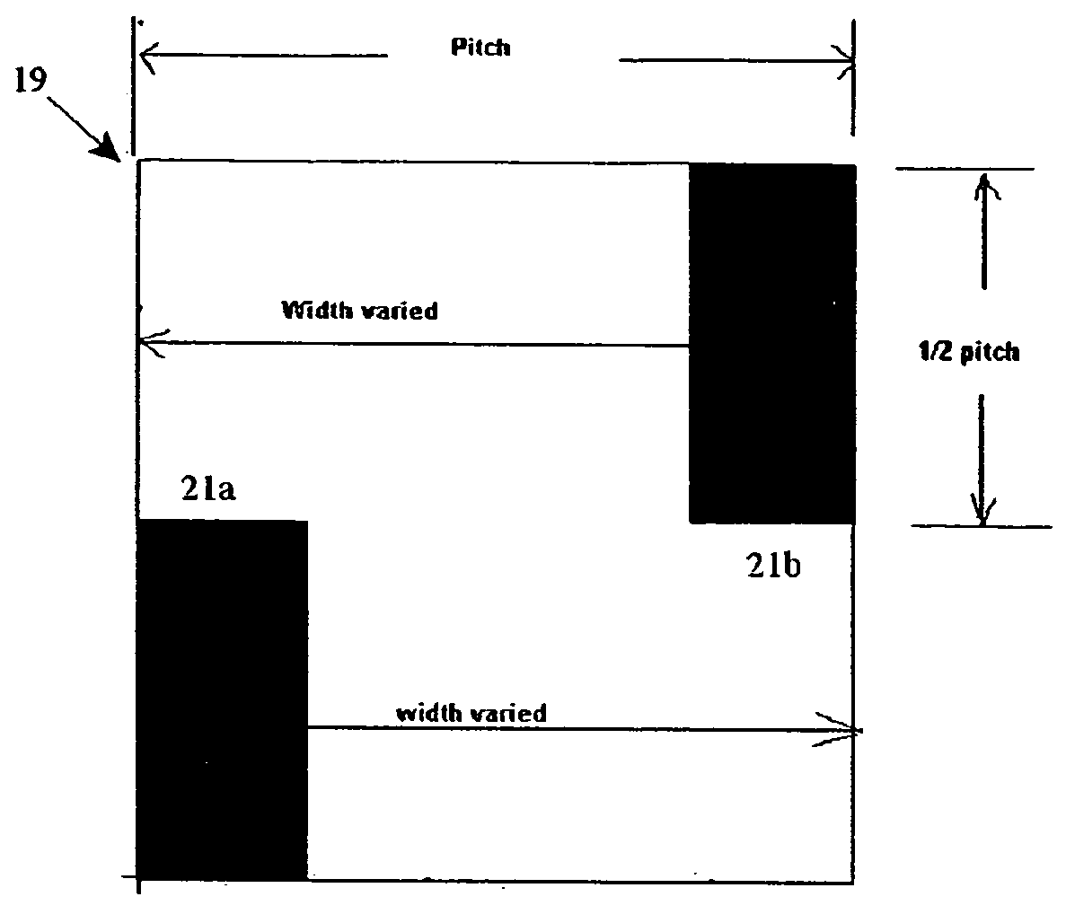
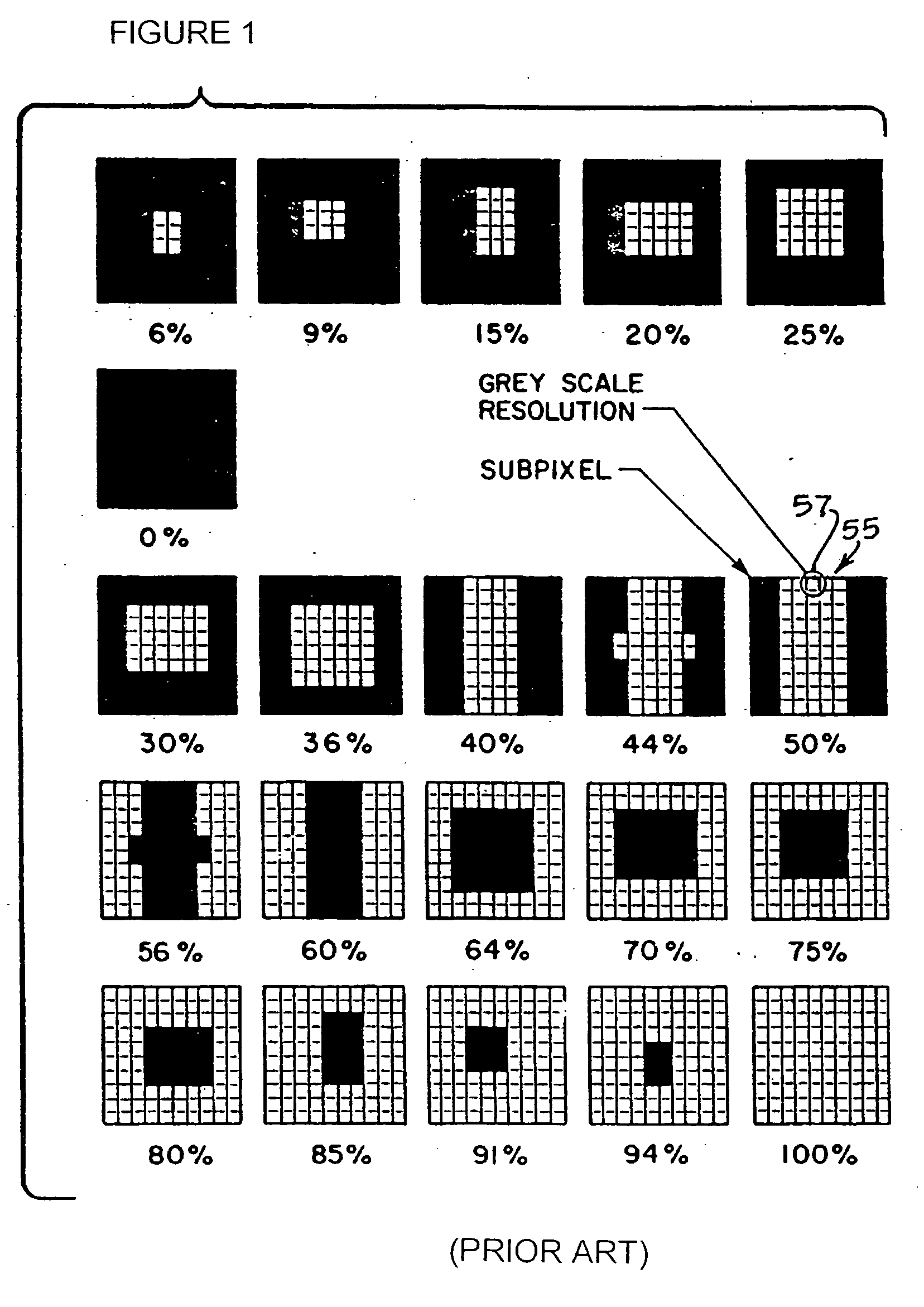
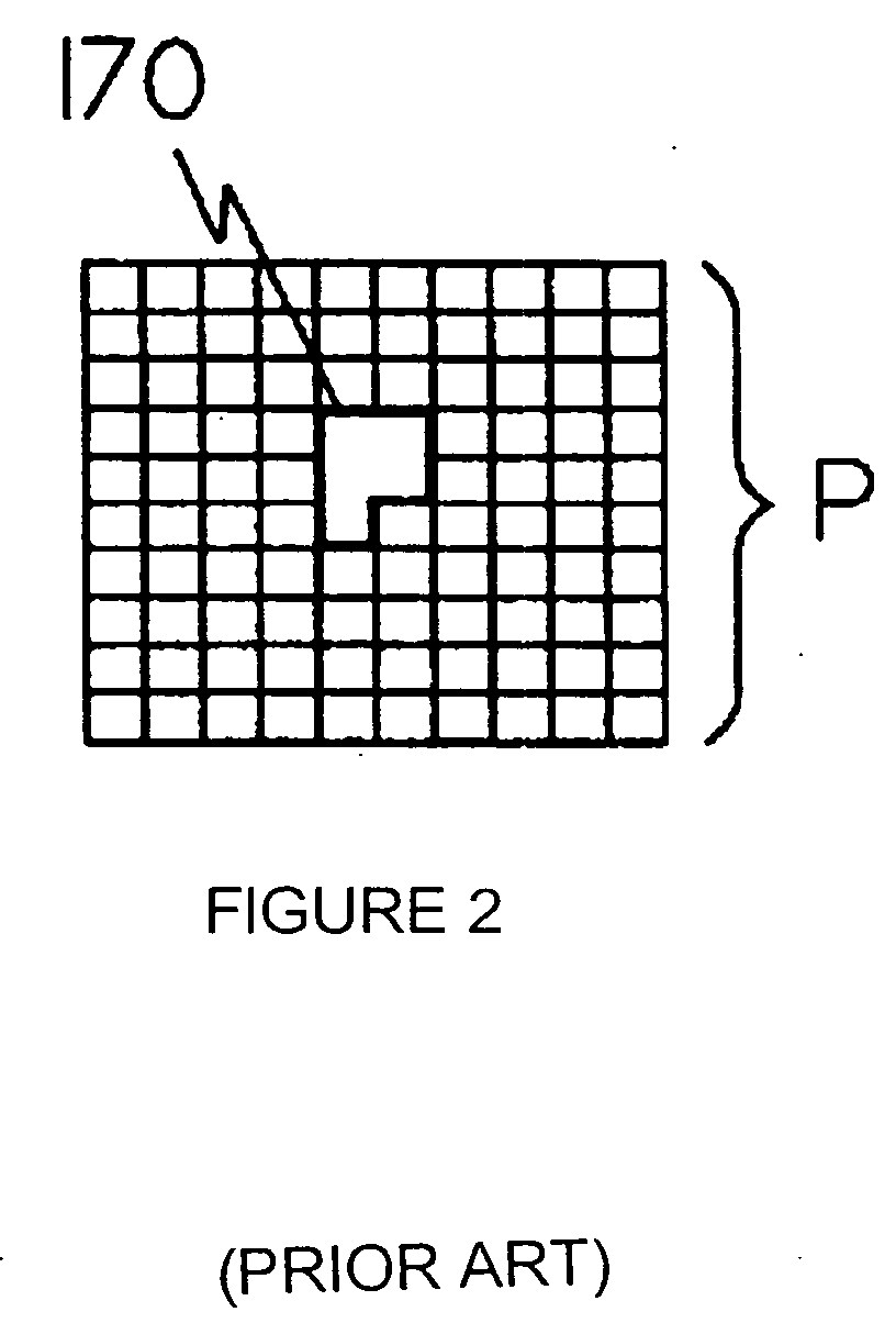
[0047] The present invention generally relates to improved BHT photomasks and microscopic three-dimensional structures made from such photomasks. The present invention is also directed toward a method for designing and fabricating BHT photomasks to be used in creating such microscopic three-dimensional structures (e.g., MEMS, micro-optics, photonics, micro-structures and other three-dimensional, microscopic devices). More particularly, the present provides a method for designing a BHT photomask layout, transferring the layout to a BHT photomask and fabricating three-dimensional microscopic structures using the BHT photomask designed by the method of the present invention. As will be seen below, the method of the present invention enables a photomask designer to design a BHT photomask to have continuous gray levels such that the change in light intensity between each gray level is both finite and linear. As a result, when this BHT photomask is used to make a three-dimensional microsc...


PUM


Abstract

The present invention generally relates to improved binary half tone (“BHT”) photomasks and microscopic three-dimensional structures (e.g., MEMS, micro-optics, photonics, micro-structures and other three-dimensional, microscopic devices) made from such BHT photomasks. More particularly, the present invention provides a method for designing a BHT photomask layout, transferring the layout to a BHT photomask and fabricating three-dimensional microscopic structures using the BHT photomask designed by the method of the present invention. In this regard, the method of designing a BHT photomask layout comprises the steps of generating at least two pixels, dividing each of the pixels into sub-pixels having a variable length in a first axis and fixed length in a second axis, and arraying the pixels to form a pattern for transmitting light through the pixels so as to form a continuous tone, aerial light image. The sub-pixels' area should be smaller than the minimum resolution of an optical system of an exposure tool with which the binary half tone photomask is intended to be used. By using this method, it is possible to design a BHT photomask to have continuous gray levels such that the change in light intensity between each gray level is both finite and linear. As a result, when this BHT photomask is used to make a three-dimensional microscopic structure, it is possible to produce a smoother and more linear profile on the object being made.

Description

RELATED APPLICATIONS [0001] This application is a divisional of U.S. patent application Ser. No. 10 / 349,629, filed Jan. 23, 2003.FIELD OF THE INVENTION [0002] The present invention generally relates to binary half tone (“BHT”) photomasks and three-dimensional microscopic structures (e.g., micro-electromechanical systems (“MEMS”), micro-optics, photonics, micro-structures, imprint lithography applications and other devices) and a method for designing and fabricating the same. BACKGROUND OF THE INVENTION [0003] Recent technological advances have made it possible to use three-dimensional MEMS, micro-optical devices and other micro-structures in a variety of fields, including photonics, communications, and integrated circuits. In the past, these tiny devices were fabricated using laser micro-machining tools. However, this method was time consuming and expensive, and thus, it was typically difficult for manufacturers to meet production requirements in a cost efficient manner. In this reg...

Claims


Application Information

Patent Timeline
IPC IPC(8): G03C5/00G03F1/00G03F7/00G03F9/00G06F17/50G06K15/00H01LH01L21/027H04N1/405
CPCB82Y10/00B82Y40/00G03F7/0005G03F1/144G03F7/0002G03F1/14G03F1/50G03F1/62G03F1/38G03F9/00G03C5/00
Inventor PROGLER, CHRISTOPHER J.RHYINS, PETER
Owner PHOTRONICS INC
Why Eureka
Try Eureka