Vertical cavity surface emitting laser diode and method for manufacturing the same
a laser diode and vertical cavity technology, applied in lasers, semiconductor lasers, solid-state devices, etc., can solve the problems of difficult manufacturing of devices having such structures, increased reflectance of polarized waves reflecting mirrors in specific orientations or directions, and inherently lack of strong polarization anisotropy of vcsel, etc., to achieve excellent controllability of polarization modes, improve mass productivity, and high performan
- Summary
- Abstract
- Description
- Claims
- Application Information
AI Technical Summary
Benefits of technology
Problems solved by technology
Method used
Image

Examples
first embodiment
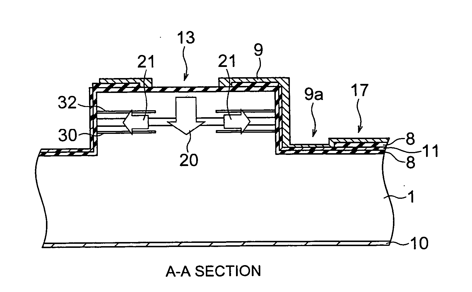
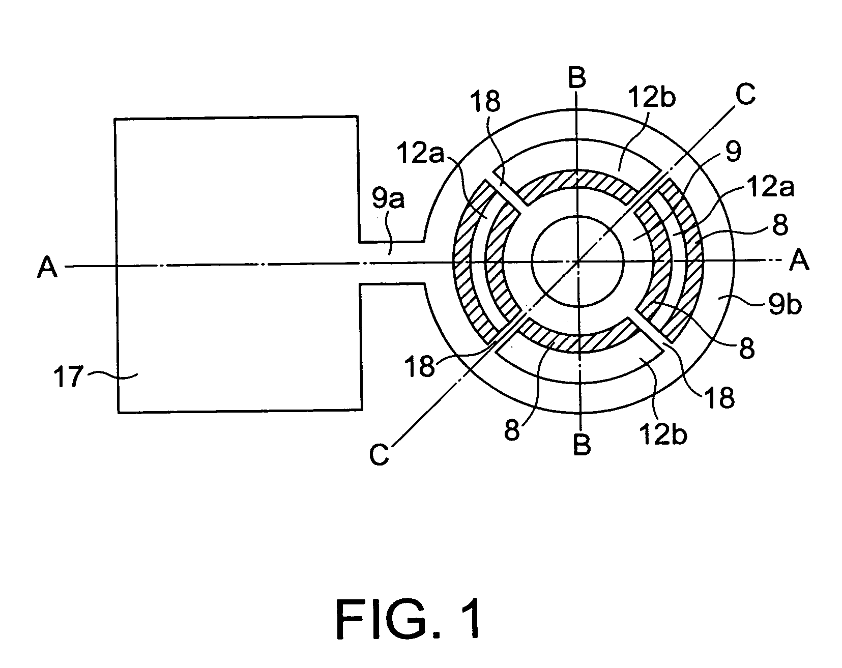
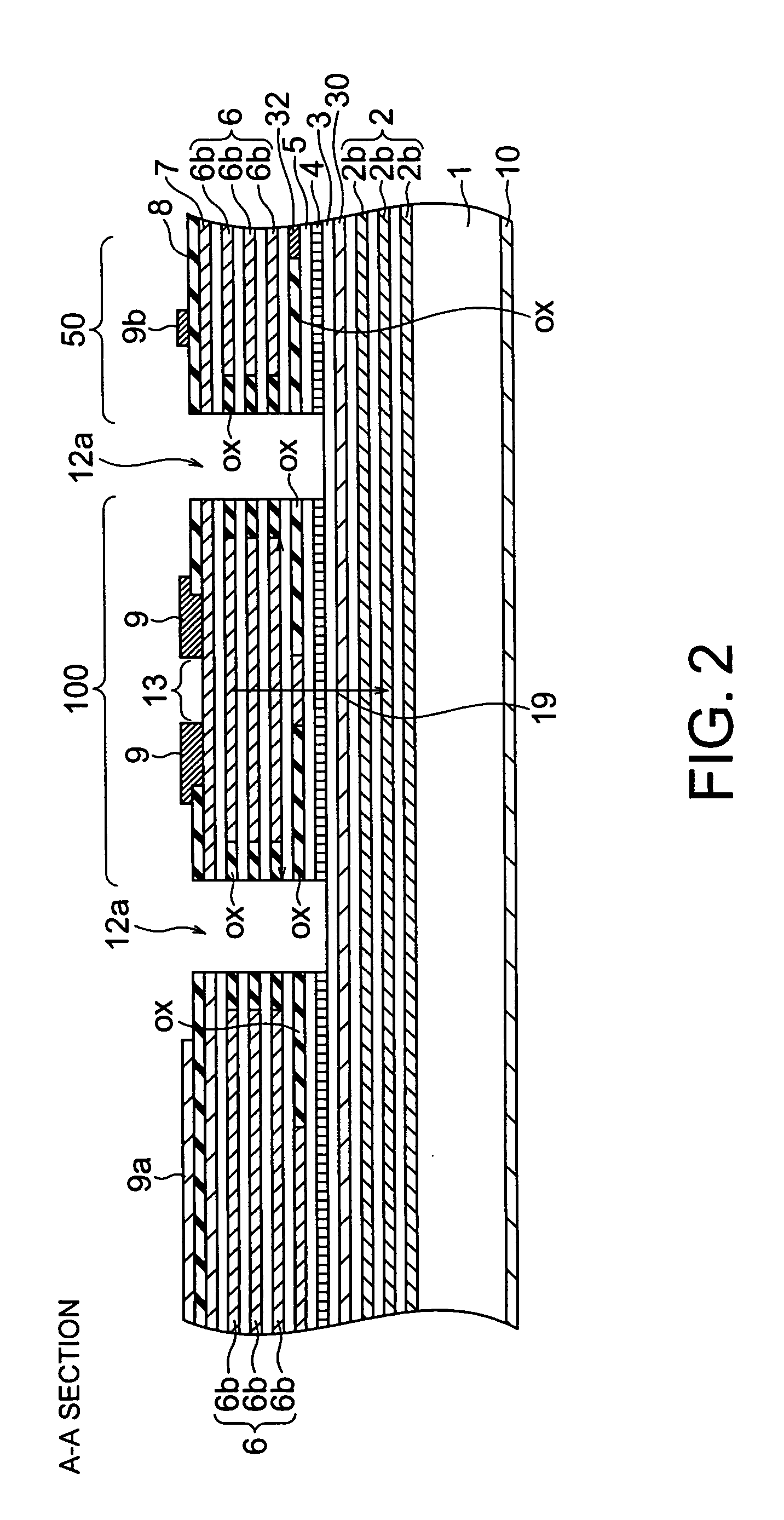
[0052] FIGS. 1 to 4 are illustrative views of a structure of a vertical cavity surface emitting laser (VCSEL) diode according to a first embodiment of the invention, FIG. 1 being a top view thereof, and FIGS. 2 to 4 being sectional views thereof taken along line A-A, line B-B and line C-C shown in FIG. 1, respectively. That is, FIG. 2 is a sectional view of the VCSEL diode where only an upper layer 32 to be selectively oxidized has been selectively oxidized, FIG. 3 is a sectional view thereof where the upper layer 32 and a lower layer 30 to be selectively oxidized have been selectively oxidized, and FIG. 4 is a sectional view of a mesa portion 100 positioned below a wire path 18.
[0053] The VCSEL diode has a semiconductor active layer 4, a first semiconductor multi-layered reflecting mirror 6 formed on a top of the semiconductor active layer 4, and a second semiconductor multi-layered reflecting mirror 2 formed under the semiconductor active layer 4 on a substrate 1 with a non-off-a...
second embodiment
[0099] FIGS. 12 to 15 are illustrative views of a structure of a VCSEL diode device according to a second embodiment of the invention, FIG. 12 being a top view thereof, FIG. 13 being a sectional view thereof taken along line A-A shown in FIG. 12, and FIG. 14 being a sectional view thereof taken along line B-B shown in FIG. 12. FIG. 15 is an enlarged sectional view of a mesa central portion shown in FIG. 14. Here, a VCSEL diode will also be explained.
[0100] In a VCSEL diode of this embodiment, the semiconductor active layer 4, the first semiconductor multi-layered reflecting mirror 6 and the second semiconductor multi-layered reflecting mirror 2 are formed on the substrate 1 like the first embodiment. The first semiconductor multi-layered reflecting mirror 6 is provided on the opposite side of the semiconductor active layer 4 from the substrate 1. The second semiconductor multi-layered reflecting mirror 2 is provided on a side of the substrate 1 to the semiconductor active layer 4. ...
third embodiment
[0125] Next, a third embodiment of the present invention will be explained.
[0126] FIGS. 17 to 20 are illustrative views of a VCSEL diode according to a third embodiment of the invention, FIG. 17 being a plan view thereof, FIG. 18 being a sectional view thereof taken along line A-A shown in FIG. 17, and FIG. 19 being a sectional view thereof taken along line B-B shown in FIG. 17, and FIG. 20 being a sectional view thereof taken along line C-C shown in FIG. 17. In these figures, constituent elements similar to those described regarding FIGS. 1 to 16 are denoted by similar reference numerals, and detailed explanation thereof will be omitted.
[0127] A current confinement portion is formed by oxidizing the layer to be oxidized 32 containing Al at a high concentration below the first semiconductor multi-layered reflecting mirror 6 from the side wall of the mesa portion 100 toward the light emitting region 13 laterally. The current confinement portion is for confinement current into the l...
PUM
 Abstract
Description
Claims
Application Information
 - R&D
- Intellectual Property
- Life Sciences
- Materials
- Tech Scout
- Unparalleled Data Quality
- Higher Quality Content
- 60% Fewer Hallucinations
Browse by: Latest US Patents, China's latest patents, Technical Efficacy Thesaurus, Application Domain, Technology Topic, Popular Technical Reports.
© 2025 PatSnap. All rights reserved.Legal|Privacy policy|Modern Slavery Act Transparency Statement|Sitemap|About US| Contact US: help@patsnap.com