Method and apparatus for reviewing defects

a technology of defects and inspection methods, applied in material analysis, material analysis, instruments, etc., can solve problems such as short circuit defects of wiring, capacitor insulation defects, and insulation defects, and achieve the effect of improving the throughput of sem-aided close inspection

Inactive Publication Date: 2005-06-09
HITACHI HIGH-TECH CORP
View PDF8 Cites 63 Cited by
  • Summary
  • Abstract
  • Description
  • Claims
  • Application Information

AI Technical Summary

Benefits of technology

[0013] According to the present invention, when the defects detected with an optical type of extraneous substance inspection apparatus or an optical-type visual inspection apparatus are to be close

Problems solved by technology

In semiconductor-manufacturing processes, the presence of foreign particle on semiconductor substrate (wafer) causes insulation defect and short circuit defect of wiring.
In addition, as semiconductor elements are followed on being formed super minute pattern, superfine foreign particles also cause insulation defects in capacitors and the destruction of gate oxide films or the like.
For this reason, large-error components are contained in the accuracy of the position coordinates calculated from the position of the laser beam spot scanning the surface of the semiconductor substrate.
In such a case, althou

Method used


Image

  • Method and apparatus for reviewing defects
  • Method and apparatus for reviewing defects
  • Method and apparatus for reviewing defects

Examples


Embodiment Construction

[0029] Embodiments of the present invention are described below using the accompanying drawings.

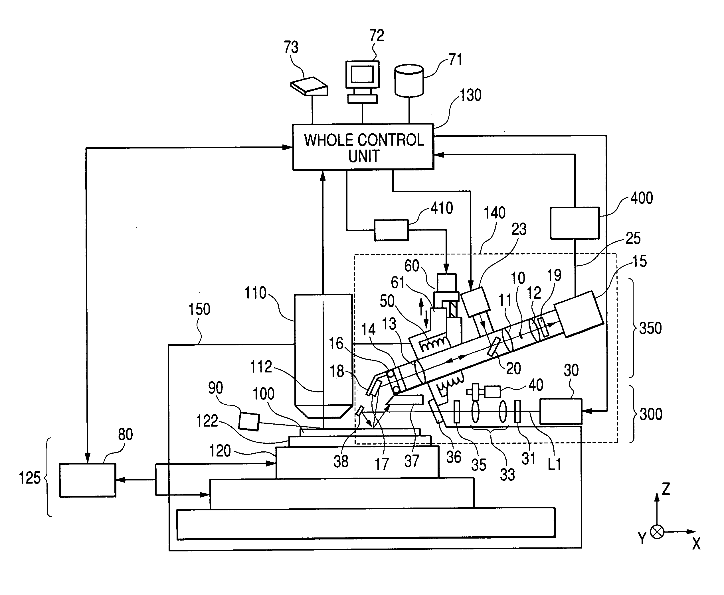
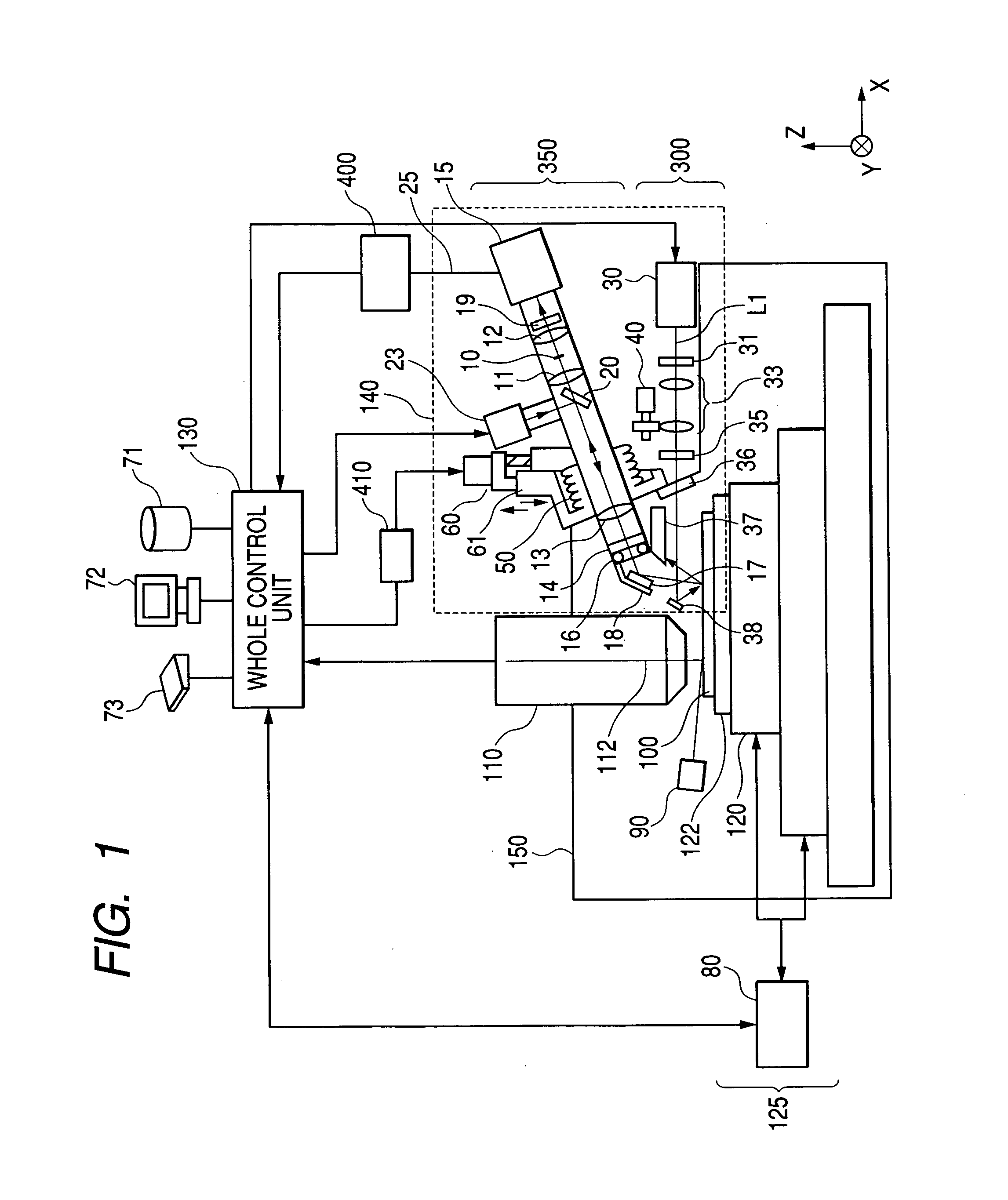
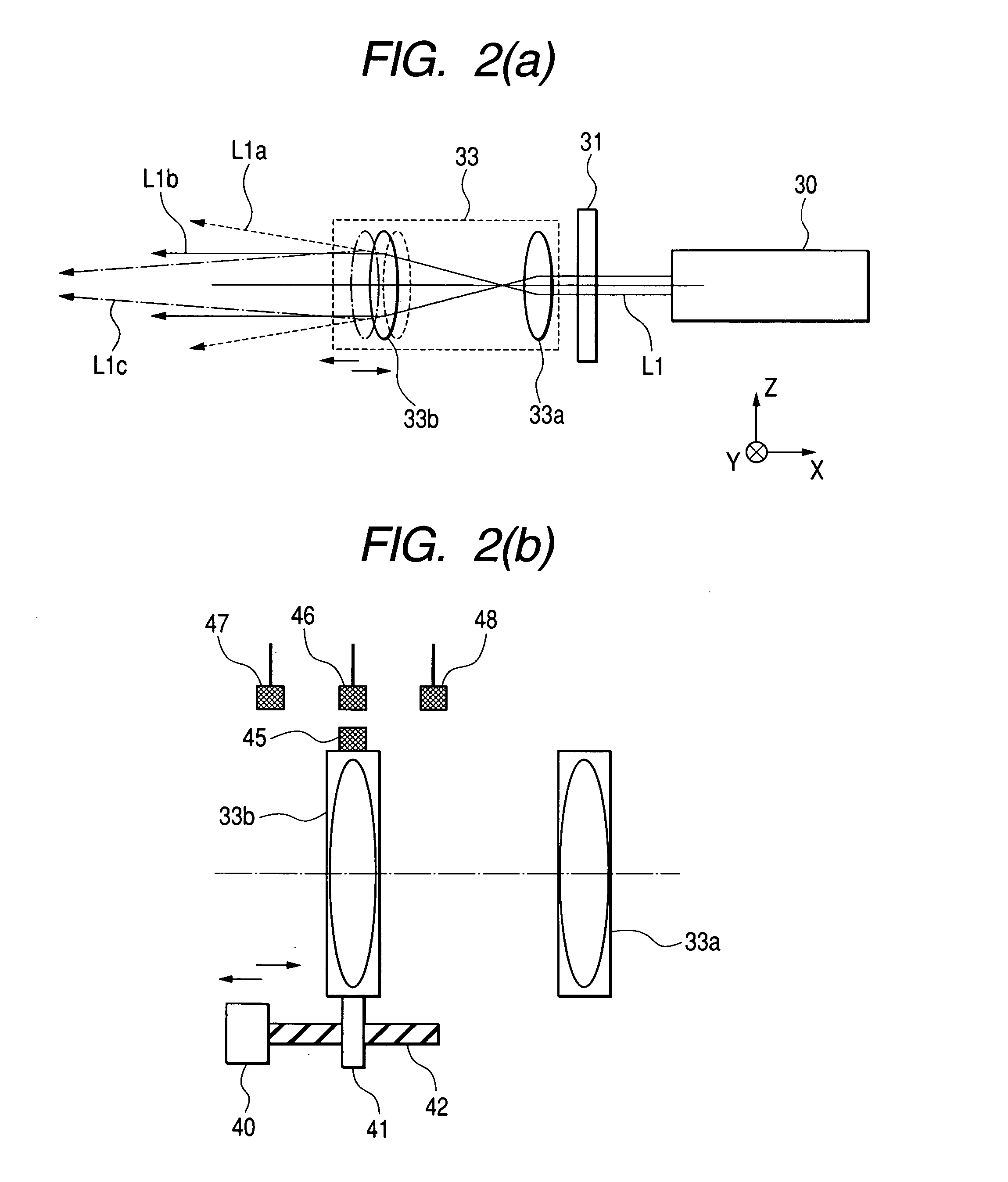
[0030] As shown in FIG. 1, the object surface defect inspection apparatus constructed according to the present invention includes: a transfer system 125 equipped with an XY stage 120 for resting and moving a substrate 100 to be inspected (such as any one of the wafers obtained from a variety of product types and manufacturing processes), and with a controller 80, a dark-field illumination system 300 that sets the laser light L1 emitted from a laser light source 30, to a size via a beam diameter-changing element 33 and then provides irradiation from a diagonally upward direction of the substrate 100 via a retardation plate (½λ plate) (what rotates the polarization direction 90 degrees) 35 and a mirror 38, a defect detection device 140 that has a detection optical system 350 including objective lenses 13, a beam splitter 20, a first lens group 11, a spatial filter 10, a second lens group 1...


PUM


Abstract

The present invention provides an apparatus capable of, and a method for, inspecting at high speed and with high accuracy the super minute foreign particles and pattern defects occurring during device-manufacturing processes in which circuit patterns are to be formed on a sample such as a substrate of semiconductor devices and other elements: in the invention, the sample is illuminated in a dark field from multiple directions each of a different incident angle, the light scattered from the sample during the dark-field illumination is detected in each of the multiple directions, and the signals obtained by detecting the scattered light in each direction; thus, defects present on the surface of an optically transparent film of the sample, and defects present in or under the transparent film are discriminated from each other and both types of defects are discriminatively reviewed using a scanning electron microscope.

Description

BACKGROUND OF THE INVENTION [0001] The present invention relates to a method and apparatus for inspecting the defects occurring in semiconductor-manufacturing processes, and more particularly, to a method and apparatus suitable for closely reviewing defects using a scanning electron microscope. [0002] In semiconductor-manufacturing processes, the presence of foreign particle on semiconductor substrate (wafer) causes insulation defect and short circuit defect of wiring. In addition, as semiconductor elements are followed on being formed super minute pattern, superfine foreign particles also cause insulation defects in capacitors and the destruction of gate oxide films or the like. These foreign particles enter in the semiconductor wafer in various states by various reasons (various causes) such as origination from the movable section of a transfer apparatus, origination from the human body, production by reaction inside a processing apparatus due to process gas usage, or entrainment ...

Claims


Application Information

Patent Timeline
IPC IPC(8): G01N21/956G01N23/225
CPCG01N21/956H01J2237/2482H01J37/226G01N23/2251
Inventor UTO, SACHIOOHSHIMA, YOSHIMASANOGUCHI, MINORIKUROSAKI, TOSHIEI
Owner HITACHI HIGH-TECH CORP
Why Eureka
Try Eureka