Device and method for anisotropically plasma etching of a substrate, particularly a silicon body

a technology of anisotropic etching and substrate, which is applied in the direction of decorative surface effects, electrical appliances, decorative arts, etc., can solve the problems of reducing mask selectivity, increasing the risk of undesirable roughness in the etching base, and so on, so as to avoid process instabilities and smooth the sidewall of the trench

Inactive Publication Date: 2005-06-16
ROBERT BOSCH GMBH
View PDF6 Cites 29 Cited by
  • Summary
  • Abstract
  • Description
  • Claims
  • Application Information

AI Technical Summary

Benefits of technology

[0010] The exemplary device according to the present invention and the exemplary method according to the present invention have the advantage that a constant change between the etching gas and the passivation gas within the plasma etching device may be dispensed with, thus avoiding the process instabilities associated therewith and overall even smoother sidewalls of the trenches created are achieved. At the same time, the advantages of the method according to German patent document no. 42 41 045 are maintained and the process parameters and installation configurations developed for it may still be used, apart from the manner of defining the etching gas and passivation gas zones which are provided in a novel manner. Consequently, the exemplary device according to the present invention may easily be integrated into an existing installation, and the exemplary method according to the present invention may still be followed based on the method according to German patent document no. 42 41 045, without major investment or the development of completely new process parameters.
[0011] The exemplary method of the present invention makes provides for achieving vertical and very smooth etching profiles, in particular in silicon, in a continuous process, at very high etching rates. In particular, visually smooth sidewalls may be produced, as required for optical components such as micro-mirrors. At the same time, a higher level of structuring accuracy is achieved with reduced critical dimension loss, which will become more and more important for microsensors in future.
[0012] Thus, it is advantageous if a certain proportion of oxygen is added to the etching gas SF6 flowing through the etching gas zones used to generate the fluorine radicals, as in German patent document no. 198 26 382. This added oxygen does not bring about any damaging influence on the process but ensures that sulfur compounds react to SO2 and similar volatile substances instead of being precipitated out as a long-chain polymer-like sulfur film in the outgoing gas region of the plasma etching system.
[0013] It is furthermore advantageous, in particular when ceramic materials are used for the reactor of the plasma etching device, if a relatively small quantity of oxygen is also added to the passivation gas flowing through the passivation gas zones used to generate Teflon-forming monomers, in order to suppress the creation of graphite particles which could act as damaging micro-masks on the semiconductor substrate to be etched, which is typically in the form of a silicon wafer. For the oxygen portion in the passivation gas to remain harmless with respect to the process, the oxygen quantities used there are typically restricted to approximately 10% to 20% of the oxygen value added or capable of being added to the etching gas. When quartz glass or another glass is used as the reactor material, this addition of oxygen is not usually necessary, since no graphite particles form on glass surfaces because of the chemically bonded oxygen there.

Problems solved by technology

If the attempt is made to supply a plasma having fluorine-donating etching gases and polymer-forming passivation gases at the same time and to break these up therein in order to generate a high density of etching species and passivation species at the same time, then a damaging mutual influence and undesirable recombination of both species is observed; this means that instead of polymer films being formed on the side walls and efficient etching being carried out at the etching base, the fluorine radicals and the polymerizable Teflon formers react to form saturated fluorine compounds which are largely inactive with respect to silicon.
However, this approach results, referring to the Si etching rate achievable per kilowatt of plasma output, in relatively inefficient processes and is problematic with regard to profile control and the reactor contamination with polymers which occurs at the same time and which is primarily caused by the required excess of passivation gas compared with the etching gas.
However, it is disadvantageous here that side wall passivation is brought about by comparatively hard films similar to SiO2 which require a higher energy input through a directed ion bombardment in order to be capable of being broken through on the etching base, and this greatly reduces mask selectivity.
The etching process according to U.S. Pat. No. 6,303,512 therefore has to operate while taking into account the limits in view of mask selectivity, which increases the risk of undesirable roughness in the etching base and so-called “grassing”.
Passivation with the aid of SiO2 also has the disadvantage that inhomogeneities in the energy input to the etched substrate bring about much more pronounced disruptive effects than in the case of Teflon-like films.
The problem here is the limited plasma stability during gas change, where changes in impedance in the plasma may result in a mismatch of the high-frequency or microwave radiation supplied, which gives rise to reflected output until the plasma discharge begins (“flickering”).
Moreover, this process sometimes involves individual cases in which it may not be possible to make the sidewalls of the trenches created completely smooth, which may be disadvantageous for example for optical applications using mirror surfaces.

Method used


Image

  • Device and method for anisotropically plasma etching of a substrate, particularly a silicon body
  • Device and method for anisotropically plasma etching of a substrate, particularly a silicon body
  • Device and method for anisotropically plasma etching of a substrate, particularly a silicon body

Examples


Embodiment Construction

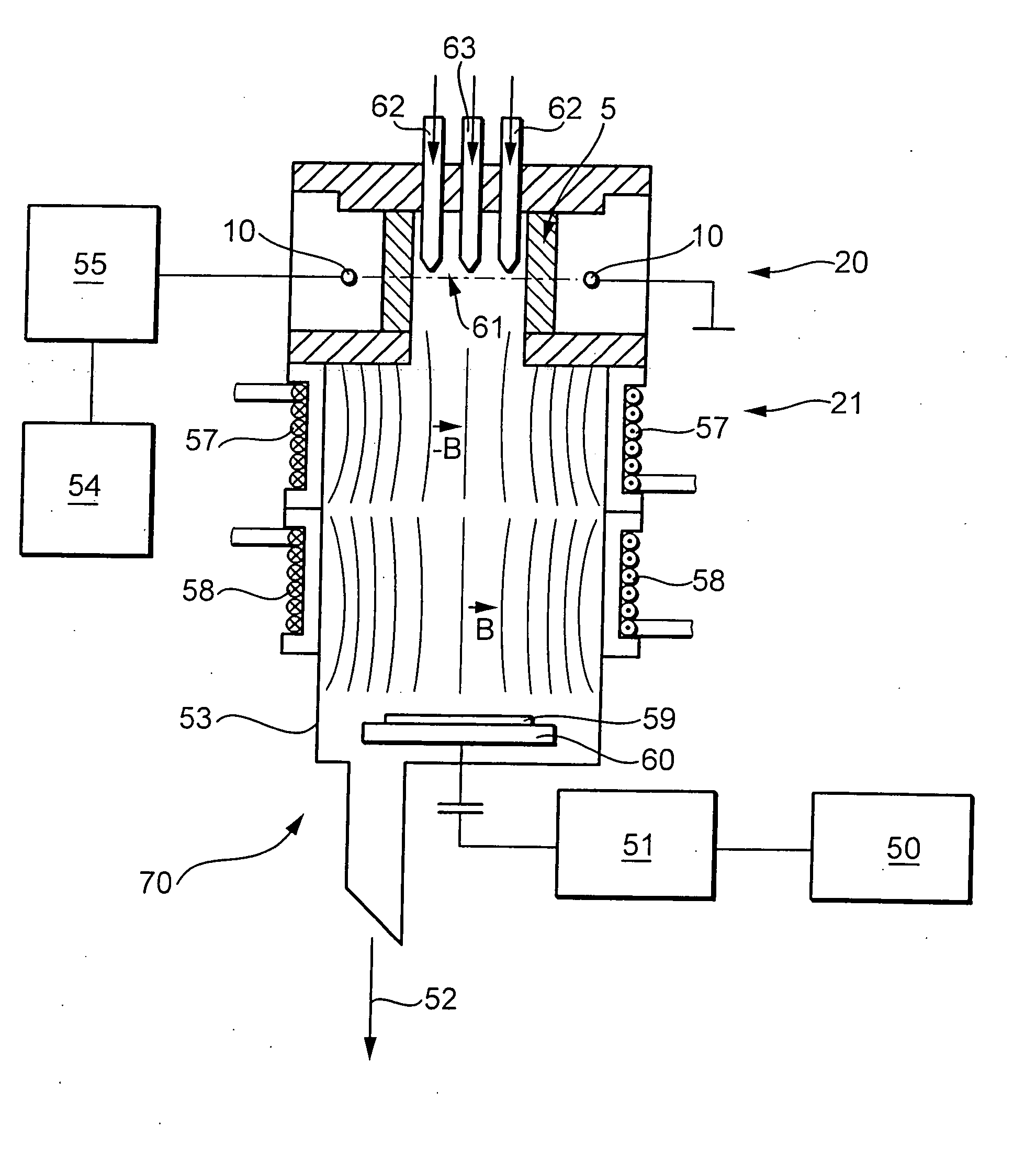
[0029] The exemplary device according to the present invention and the exemplary method according to the present invention, which may be implemented using the method, have the principal aim, instead of providing a separation in time between generating an etching species (F) which etches silicon, for example, and a passivation species (CnF2n) forming Teflon-like films, as from German patent document no. 41 42 045, to provide physical separation between the locations where the two species in the plasma etching system are generated in order to be able to generate them at the same time and as far as possible without damaging interactions between them. However, it should be stressed that time separation as well as physical separation may be achieved; i.e., the exemplary embodiment and / or exemplary method according to the present invention may also be combined with the procedure according to German patent document no. 42 41 045 where required. However, this is not typically necessary.

[00...


PUM

PropertyMeasurementUnit
frequencyaaaaaaaaaa
pressureaaaaaaaaaa
temperatureaaaaaaaaaa

Abstract

A method and device for implementing the method for anisotropically plasma etching a substrate (e.g., silicon body). The device has a chamber and plasma source for generating a high-frequency electromagnetic alternating field and a reaction region for generating a plasma having reactive species, within the chamber, that is generated by the action of the alternating field on etching gas and passivation gas introduced at the same time but spatially separated from it. An arrangement defines at least one first zone acted on by the etching gas and at least one second zone acted on by the passivation gas in the reaction region. The device has a mixing region downstream of the reaction region in which the reactive species generated from the etching gas in the first zone and the reactive species generated from the passivation gas in the second zone are blended before they act on the substrate.

Description

FIELD OF THE INVENTION [0001] The present invention relates to a device and a method for anisotropic etching of a substrate, a silicon body in particular, using a plasma source. BACKGROUND INFORMATION [0002] When silicon is subjected to high-rate anisotropic plasma etching using the maximum possible mask selectivity and the best possible profile control, for example in the manner referred to in German patent document no. 42 41 045, a stable passivation which can easily be removed again from the etching base of the structures to be etched while maintaining the mask selectivity, i.e., as a result of ion bombardment with a low energy input per unit of time, has to be applied to the side walls of the structures to be etched. At the same time, a high density of etching species has to be provided for removing the silicon from the etching base. [0003] Fluorine radicals from fluorine-donating etching gases such as SF6, NF3, ClF3, BrF3, etc., which are broken up in a high-density plasma, are...

Claims


Application Information

Patent Timeline
Patent Type & Authority Applications(United States)
IPC IPC(8): H01L21/00
CPCH01L21/67069
Inventor LAERMER, FRANZBREITSCHWERDT, KLAUSKUTSCH, BERND
Owner ROBERT BOSCH GMBH
Why Eureka
Try Eureka