Method for making metal capacitors with low leakage currents for mixed-signal devices

a technology of mixed-signal devices and metal capacitors, which is applied in the direction of capacitors, variable capacitors, electrical appliances, etc., can solve the problems of lower breakdown voltage and higher leakage current of high-k dielectrics, and achieve low leakage current and high capacitance per unit area

Inactive Publication Date: 2005-06-23
TAIWAN SEMICON MFG CO LTD
View PDF16 Cites 54 Cited by
  • Summary
  • Abstract
  • Description
  • Claims
  • Application Information

AI Technical Summary

Benefits of technology

[0013] A principal object of the present invention is to provide a metal-insulator-metal capacitor comprised of a sandwiched layer of a wide-band-gap oxide, a

Problems solved by technology

Unfortunately, these high-k dielectrics have a hi

Method used


Image

  • Method for making metal capacitors with low leakage currents for mixed-signal devices
  • Method for making metal capacitors with low leakage currents for mixed-signal devices
  • Method for making metal capacitors with low leakage currents for mixed-signal devices

Examples


Embodiment Construction

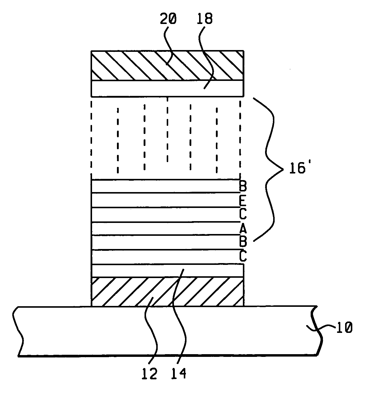
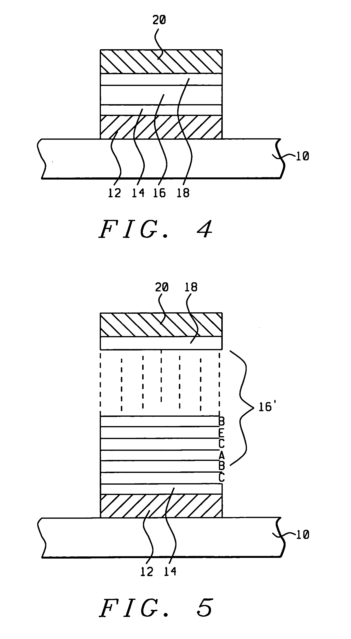
[0022] The present invention relates to a method for making metal-insulator-metal (MIM) capacitors on a partially completed substrate having devices. Typically the substrate is a semiconductor material, such as a doped single-crystal silicon, gallium arsenide, or the like. After forming semiconductor devices, such as FETs, bipolar transistors, and the like in and on the substrate, the devices are insulated, and the MIM capacitors are formed having electrical connections to the devices.

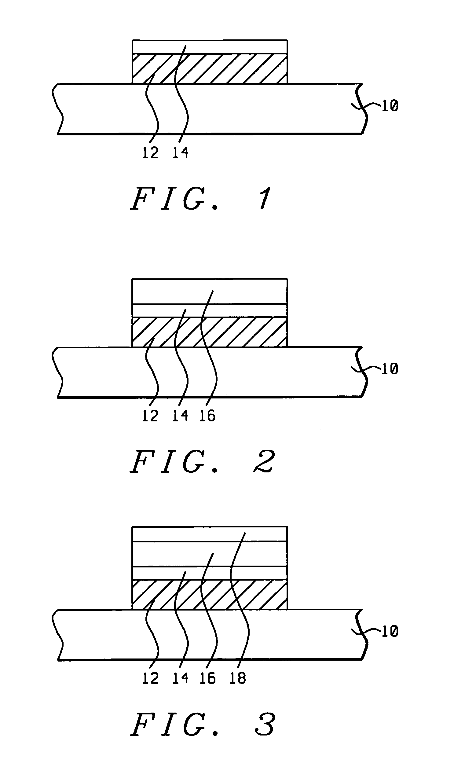
[0023] Referring first to FIG. 1, a schematic cross-sectional view is shown of a portion of a semiconductor substrate 10 having devices (not shown). By a first embodiment of this invention, the method for making the MIM capacitors begins by depositing a first conducting layer. The first conducting layer is then patterned to form the capacitor bottom electrodes 12. The first conducting layer is preferably titanium nitride (TiN), deposited, for example, by physical vapor deposition such as by sputtering...


PUM

PropertyMeasurementUnit
Temperatureaaaaaaaaaa
Timeaaaaaaaaaa

Abstract

A method for making metal-insulator-metal (MIM) capacitors having insulators with high-dielectric-constant and sandwiched between wide-band-gap insulators resulting in low leakage currents and high capacitance per unit area is achieved. The high-k layer increases the capacitance per unit area for next generation mixed-signal devices while the wide-band-gap insulators reduce leakage currents. In a second embodiment, a multilayer of different high-k materials is formed between the wide-band-gap insulators to substantially increase the capacitance per unit area. The layer materials and thicknesses are optimized to reduce the nonlinear capacitance dependence on voltage.

Description

[0001] This patent application is a continuation in part of U.S. patent application Ser. No. 09 / 992,458, filed on Nov. 16, 2001.BACKGROUND OF THE INVENTION [0002] (1) Field of the Invention [0003] The present invention relates to a method for making multilayer metal-insulator-metal capacitors for ultra-large-scale integration (ULSI), and more particularly relates to a method for making small metal capacitors with increased capacitance per unit area with lower leakage currents. This sandwiched capacitor uses a high-k dielectric film having a narrow band gap sandwiched between two insulating layers having a wide band gap. This structure allows one to reduce leakage currents while also allowing one to minimize the high-order coefficients for the capacitance-versus-voltage curve and to provide capacitors with are lower voltage-dependent. [0004] (2) Description of the Prior Art [0005] Capacitors on semiconductor chips are used for various integrated circuit applications. For example, the...

Claims


Application Information

Patent Timeline
IPC IPC(8): H01L21/02H01L21/316
CPCH01L21/31604H01L28/56Y10T29/435Y10T29/43Y10T29/417H01L28/40H01L21/02263
Inventor SHIH, WONG-CHENGTING, WEN-CHILEE, TZYH-CHEANGLIN, CHIH-HSIENWONG, SHYH-CHYI
Owner TAIWAN SEMICON MFG CO LTD
Why Eureka
Try Eureka