Asymmetric MOS transistor with trench-type gate

a technology of trench-type gate and mos transistor, which is applied in the field of integrated circuits, can solve the problems of short channel effect, reduced effective channel length, and degraded gate dielectric by hot carrier injection, and achieve the effect of lengthening the channel

Active Publication Date: 2005-06-23
SAMSUNG ELECTRONICS CO LTD
View PDF5 Cites 55 Cited by
  • Summary
  • Abstract
  • Description
  • Claims
  • Application Information

AI Technical Summary

Benefits of technology

[0010] Because of such disadvantageous effects from a short channel, a MOS transistor is formed with a trench-type gate for lengthening the channel especially for a low area of the MOS transistor. Alternative terms for the trench-type gate are recess-type or groove-type gate.
[0011]FIGS. 1A to 1Q are cross-sectional views illustrating the steps of fabricating such a MOS transistor with a trench-type gate according to the prior art. Referring to FIG. 1A, a first pad oxide layer 12 and a first hard mask layer 14 are sequentially formed on a semiconductor substrate 10. Referring to FIGS. 1A and 1B, photoresist is deposited on the first hard mask layer 14, and is then patterned to partially expose the hard mask layer 14. Exposed regions of the first hard mask layer 14 are etched away to define an active device region ACT within the semiconductor substrate 10. Thereafter, the photoresist is removed.
[0012] Referring to FIGS. 1B and 1C, exposed portions of the first pad oxide layer 12 and the semiconductor substrate 10 are sequentially etched. By thus using the first hard mask layer 14 as an etch mask, a first trench T1 is formed to surround the active device region ACT within the semiconductor substrate 10.
[0013] Referring to FIGS. 1C and 1D, an insulating material 16 is formed within the first trench T1. Such insulating material 16 is formed in a thermal oxidation process with the first hard mask layer 14 and the first pad oxide layer 12 being oxidation prevention masks. Thereafter, the first hard mask layer 14 and the first pad oxide layer 12 are removed by a chemical mechanical polishing (CMP) process or an etch back process. After such planarization, a STI (shallow trench isolation) structure 16 is formed to surround the exposed active device region ACT of the semiconductor substrate 10.
[0014] Referring to FIGS. 1D and 1E, a P-type dopant is implanted at high energy with relatively low concentration into the semiconductor substrate 10 to form a channel region of the MOS transistor. This channel region is formed substantially into the semiconductor substrate 10, except the STI structure 16, and so does not have a specific reference number in the drawings.
[0015] Referring to FIGS. 1E and 1F, a second pad oxide layer 18 and a second hard mask layer 20 are sequentially formed on the semiconductor substrate 10. Referring to FIGS. 1F and 1G, photoresist is deposited and patterned on the second hard mask layer 20 in a photolithography process. Thereafter, exposed portions of the second hard mask layer 20 are etched to pattern the second hard mask layer 20. Next, the photoresist is removed.

Problems solved by technology

Such reduced effective channel length and threshold voltage disadvantageously lead to short channel effects as the gate control function is degraded for the MOSFET.
However, a high electric field is applied for such a MOSFET resulting in hot carrier injection into the gate dielectric which becomes degraded.
Nevertheless with ever decreasing channel length, even the LDD structures provide limited reduction of short channel effects and hot carrier injection.
Furthermore, during operation of the MOS transistor, undesired punch-through may also occur even with such LDD structures.
Unfortunately, the prior art MOS transistor formed according to FIGS. 1A to 1Q may still exhibit short channel effects.

Method used


Image

  • Asymmetric MOS transistor with trench-type gate
  • Asymmetric MOS transistor with trench-type gate
  • Asymmetric MOS transistor with trench-type gate

Examples


Embodiment Construction

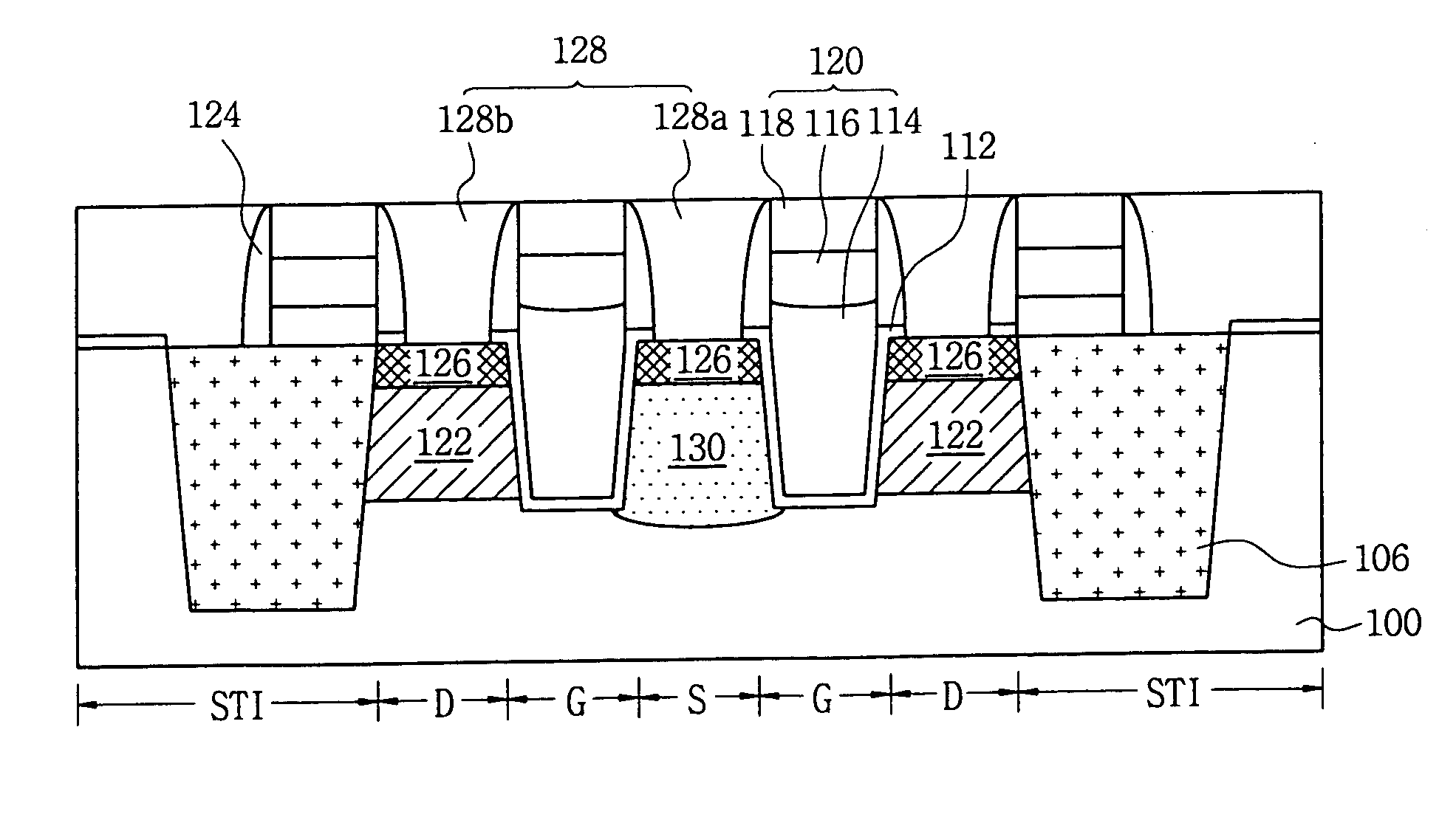
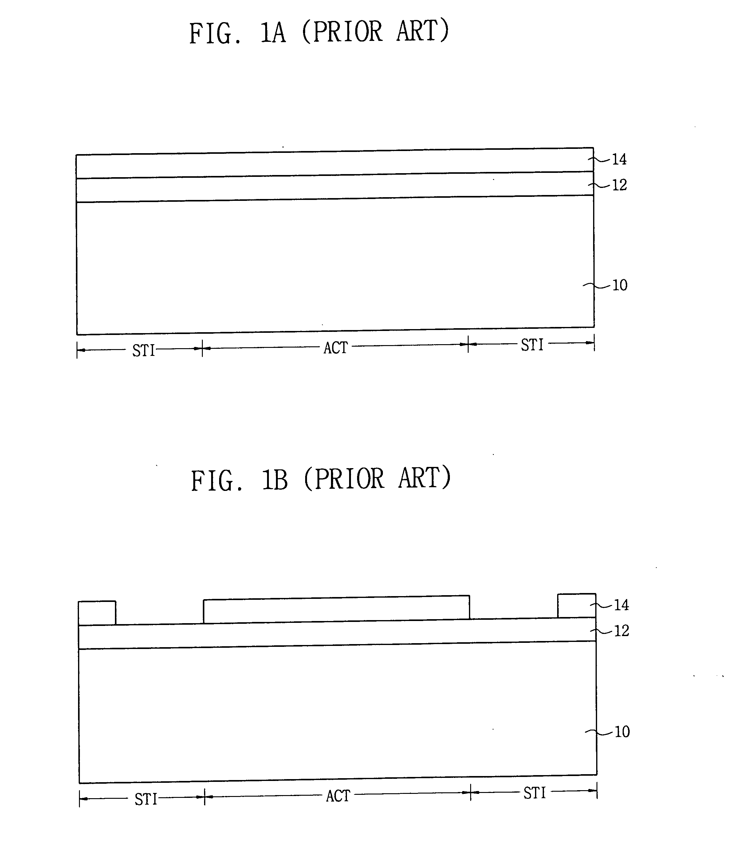
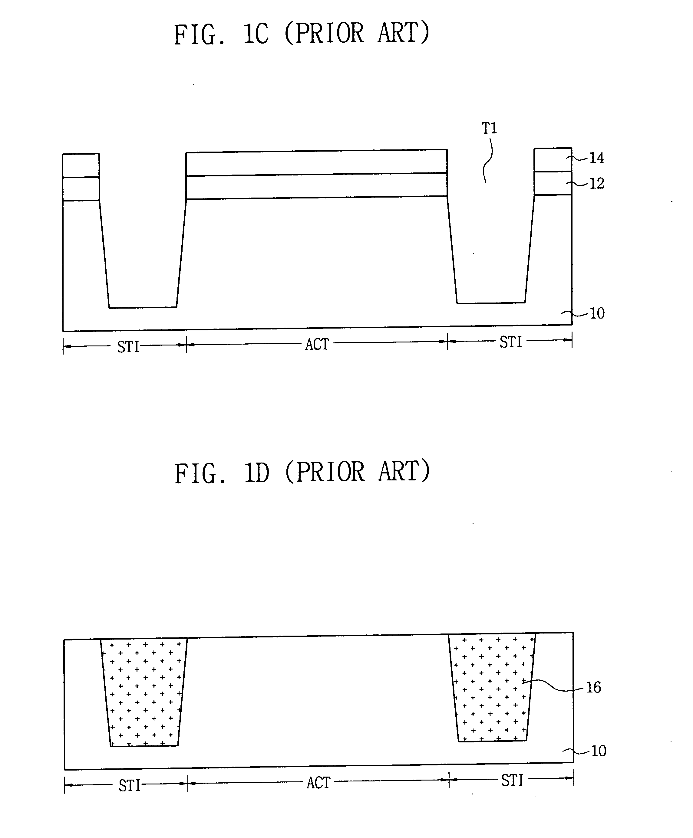
[0038]FIGS. 2A to 2R are cross-sectional views illustrating sequential steps for fabricating a MOS transistor having a trench-type gate with an asymmetric channel region, according to an embodiment of the present invention. Referring to FIG. 2A, a first pad oxide layer 102 and a first hard mask layer 104 are sequentially deposited on a semiconductor substrate 100. The first pad oxide layer 102 is formed to have a thickness of about 300 Å to about 1000 Å in an MTO (Medium Temperature Oxide) deposition process in one embodiment of the present invention.

[0039] The first hard mask layer 104 is comprised of silicon nitride or silicon oxy-nitride having a thickness of about 500 Å to about 2000 Å in one embodiment of the present invention. The first hard mask layer 104 is deposited during a chemical vapor deposition (CVD) process in one embodiment of the present invention. Though not shown in the figures, the present invention may also be practiced with a molding polysilicon layer formed ...


PUM


Abstract

a A MOS (metal oxide semiconductor) transistor with a trench-type gate is fabricated with a channel stopping region for forming an asymmetric channel region for reducing short channel effects. For example in fabricating an N-channel MOS transistor, a gate structure is formed within a trench that is within a P-well. A channel stopping region with a P-type dopant is formed to a first side of the trench to completely contain an N-type source junction therein. An N-type drain junction is formed within a LDD region to a second side of the trench, thus forming the asymmetric channel region.

Description

BACKGROUND OF THE INVENTION [0001] This application claims priority to Korean Patent Application No. 2003-0095140, filed on Dec. 23, 2003, in the Korean Intellectual Property Office, the disclosure of which is incorporated herein in its entirety by reference. [0002] 1. Field of the Invention [0003] The present invention relates generally to integrated circuits, and more particularly to fabrication of a MOS (metal oxide semiconductor) transistor with a trench-type gate and an asymmetric channel region for minimizing undesired short channel effects. [0004] 2. Description of the Related Art [0005] A MOSFET (metal oxide semiconductor field effect transistors) is a commonly used device in integrated circuits. Dimensions of integrated circuit devices are desired to be further minimized as known to one of ordinary skill in the art. The channel length of a MOSFET is reduced to deep sub-micron dimensions for enhanced operating speed and current drive capability of the MOSFET. [0006] With suc...

Claims


Application Information

Patent Timeline
Patent Type & Authority Applications(United States)
IPC IPC(8): H01L21/336H01L29/10H01L29/76H01L29/78
CPCH01L29/1045H01L29/4236H01L29/7835H01L29/66659H01L29/66621H01L21/18
Inventor SEO, HYEOUNG-WONKIM, DONG-HYUNSONG, DU-HEONLEE, SANG-HYUN
Owner SAMSUNG ELECTRONICS CO LTD
Why Eureka
Try Eureka