Method for manufacturing silicon carbide semiconductor device, and silicon carbide semiconductor device

a semiconductor device and silicon carbide technology, applied in the direction of semiconductor devices, basic electric elements, electrical apparatus, etc., can solve the problems of low channel mobility, inapplicability of techniques optimized on the (0001) plane to the (000-1) plane, and difficulty in reducing on-resistance, so as to reduce ohmic contact and high channel mobility

Active Publication Date: 2009-03-19
NAT INST OF ADVANCED IND SCI & TECH
View PDF2 Cites 17 Cited by
  • Summary
  • Abstract
  • Description
  • Claims
  • Application Information

AI Technical Summary

Benefits of technology

[0021]In accordance with this invention, since the process for fabricating a silicon carbide semiconductor device on the (000-1) plane comprises forming an insulating film by wet oxidation, terminating the interface level of the insulating film and silicon carbide with hydrogen, and subsequently performing ohmic contact anneal in a gas containing hydrogen, thereby inhibiting the hydrogen terminating the interface level of the insulating film and silicon carbide from being desorbed during the course of annealing, it is made possible to obtain high channel mobility, decrease the ohmic contact, and hence enable fabrication of a silicon semiconductor device of low on resistance.

Problems solved by technology

On this plane, however, the MOS interface reveals low mobility of channel and renders a decrease of on-resistance difficult.
Consequently, the problem that the technique optimized on the (0001) plane will not be applicable to the (000-1) plane may arise.

Method used


Image

  • Method for manufacturing silicon carbide semiconductor device, and silicon carbide semiconductor device
  • Method for manufacturing silicon carbide semiconductor device, and silicon carbide semiconductor device
  • Method for manufacturing silicon carbide semiconductor device, and silicon carbide semiconductor device

Examples


first embodiment

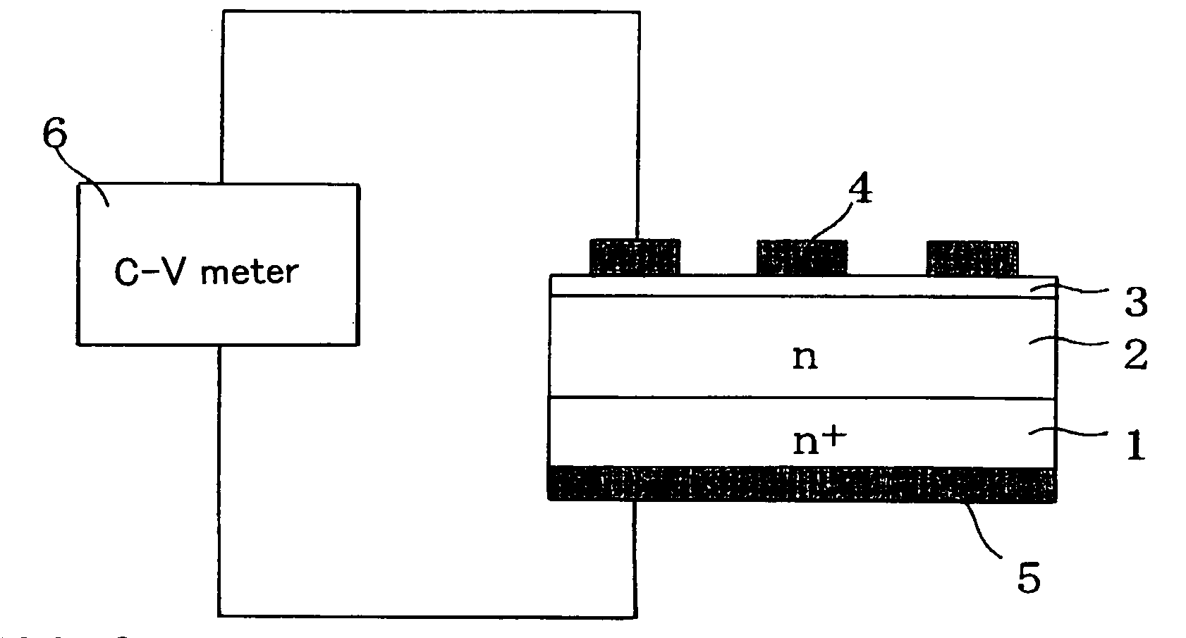
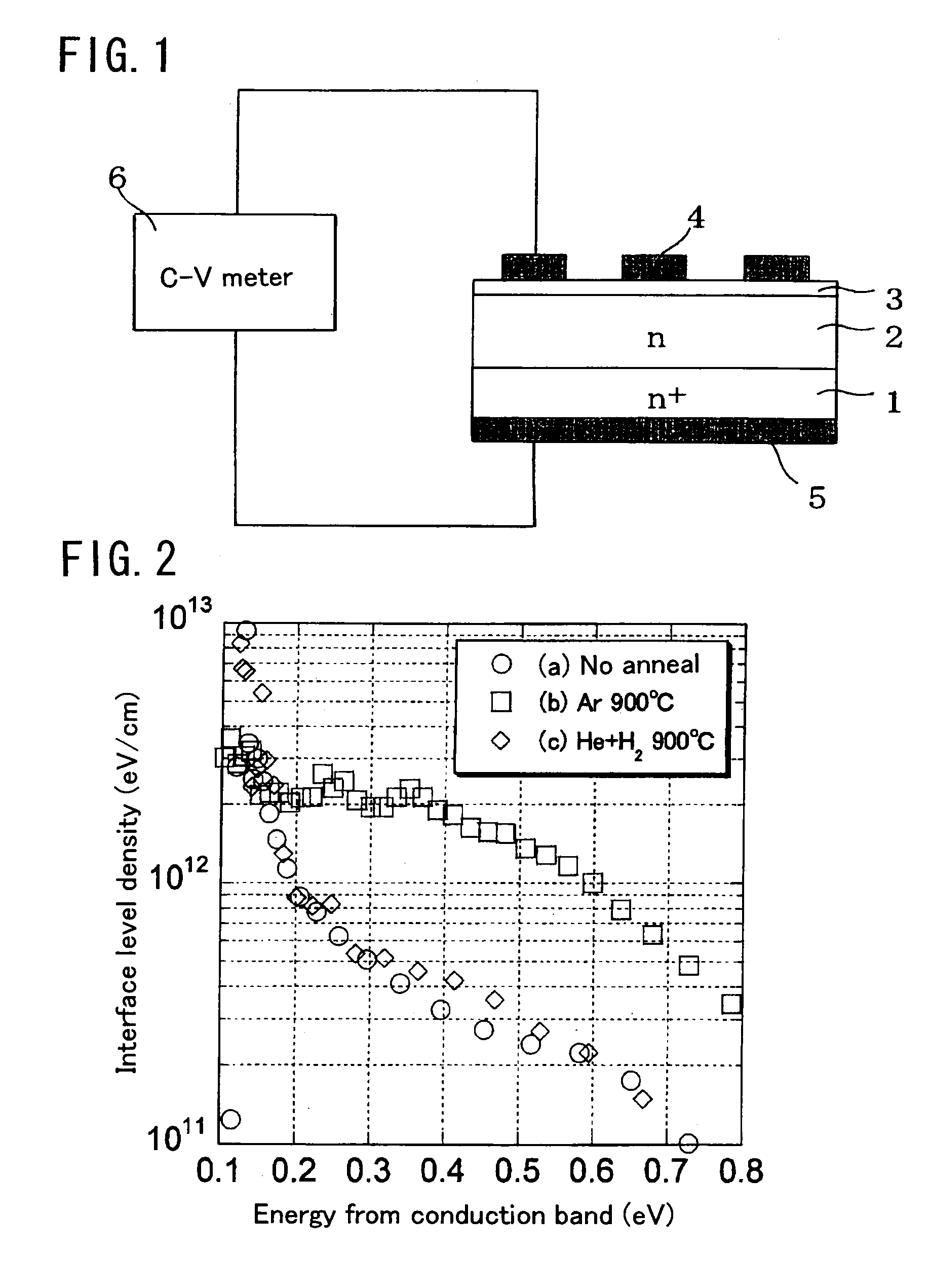
[0053]this invention will be described with reference to FIG. 1 and FIG. 2.

[0054]FIG. 1 is a diagram that depicts the structure of a MOS capacitor according to this invention.

[0055]This MOS capacitor is fabricated as follows.

[0056]First, an n-type epitaxial film 2 having a donor density of 1×1016 cm−3 is grown on a 0 to 8-degree-off substrate (preferably 0 to 1-degree-off substrate) from the (000-1) plane of an n-type 4H—SiC (000-1) substrate 1. Incidentally, the 4H—SiC substrate in a single form or the 4H—SiC substrate in combination with the epitaxial film will be called a 4H—SiC semiconductor.

[0057]After the 4H—SiC semiconductor is cleaned, it is subjected to wet oxidation at 900° C. over a period of 120 minutes to form an insulating film 3 measuring 50 nm in thickness and cooled to room temperature. The atmosphere used during the cooling may be an inert gas, such as argon or nitrogen, and the switch from the wet atmosphere to the inert gas may take place about 30 minutes prior t...

second embodiment

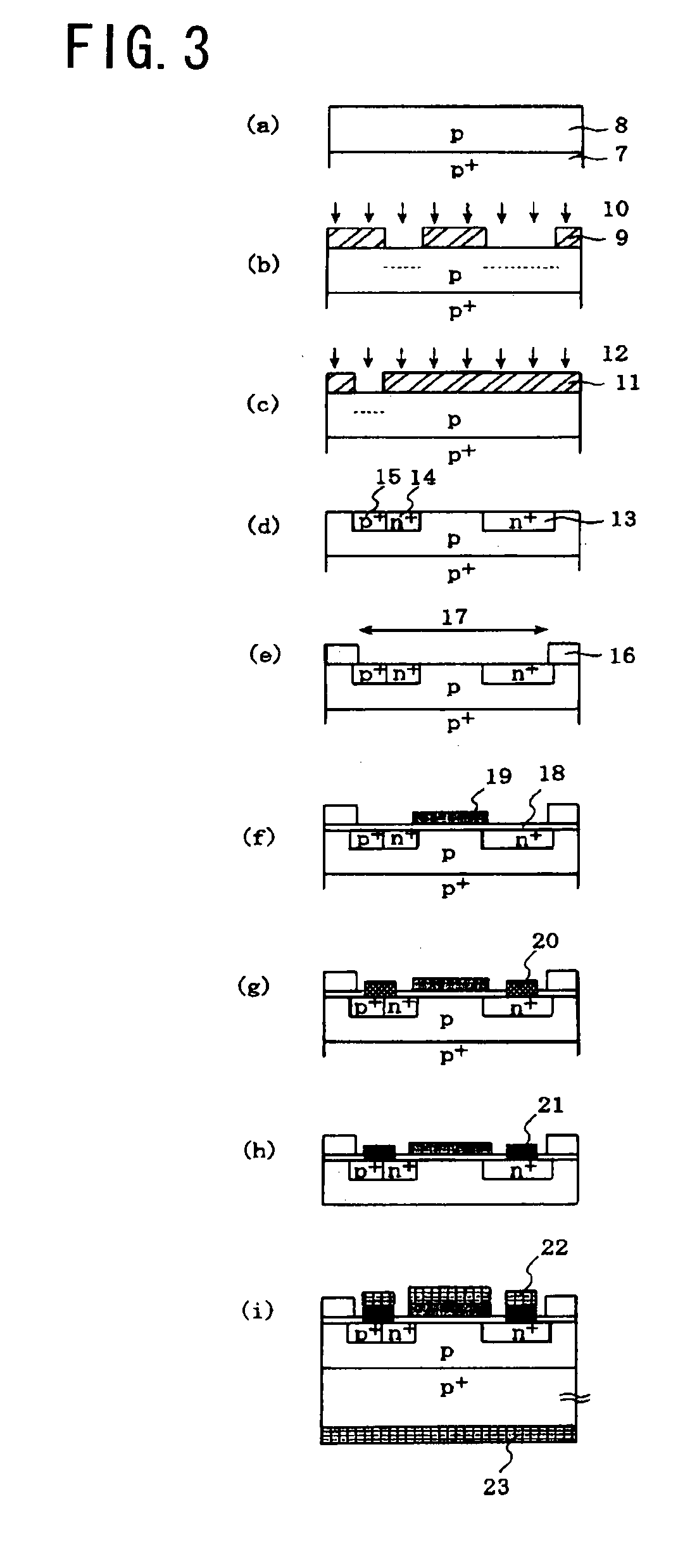
[0061]Next, this invention will be described with reference to FIG. 3 through FIG. 6.

[0062]FIG. 3 is a cross section drawn for the purpose of explaining the method of this invention for the fabrication of a MOSFET on the silicon carbide (000-11) plane.

[0063]First, a p-type epitaxial film 8 having an acceptor density of 1×1016 cm−3 is grown on a 0 to 8-degree-off substrate (preferably 0 to 1-degree-off substrate) from the (000-1) plane of a p-type 4H—SiC (000-1) substrate 1 as shown in FIG. 3(a). Incidentally, the 4H—SiC substrate in a single form or the 4H—SiC substrate in combination with the epitaxial film will be called a 4H—SiC semiconductor.

[0064]Next, as shown in FIG. 3(b), an SiO2 film measuring 1 μm in thickness is deposited on the surface of a p-type epitaxial film 8 by the low pressure CVD method and patterned by photolithography to form a mask 9. Thereafter, a phosphorus ion 10, for example, is implanted under the conditions, 500° C. in substrate temperature, 40 keV to 25...


PUM

PropertyMeasurementUnit
temperatureaaaaaaaaaa
off-angleaaaaaaaaaa

Abstract

The object is to provide a method for the fabrication of a semiconductor device having undergone an anneal treatment for the purpose of forming such ohmic contact as enables decrease of ohmic contact resistance and being provided on the (000-1) plane of silicon carbide with an insulating film and provide the semiconductor device. The method for the fabrication of a silicon carbide semiconductor device includes the steps of performing thermal oxidation on the (000-1) plane of a silicon carbide semiconductor in a gas containing at least oxygen and moisture, thereby forming an insulating film in such a manner as to contact the (000-1) plane of the silicon carbide semiconductor, removing part of the insulating film, thereby forming an opening part therein, depositing contact metal on at least part of the opening part, and performing a heat treatment, thereby forming a reaction layer of the contact metal and silicon carbide, wherein the heat treatment is implemented in a mixed gas of an inert gas and hydrogen.

Description

TECHNICAL FIELD[0001]This invention relates to a method for the fabrication of a silicon carbide semiconductor device and the silicon carbide semiconductor device and more particularly relates to a method for the fabrication of a silicon carbide semiconductor device that incorporates therein a step for forming an ohmic electrode and is provided on the (000-1) plane of a silicon carbide semiconductor with an insulating film and the silicon carbide semiconductor device.BACKGROUND ART[0002]Silicon carbide (SiC), as compared with silicon (Si), possesses excellent physical properties, such as a wide band gap and large dielectric breakdown strength. By using silicon carbide (SiC) as a substrate material, therefore, it is made feasible to fabricate a power semiconductor device of high blocking voltage and low resistance that surpass the limits of silicon (Si).[0003]Further, silicon carbide (SiC) is characterized, similarly to silicon (Si), by being capable of forming an insulating film by ...

Claims


Application Information

Patent Timeline
Patent Type & Authority Applications(United States)
IPC IPC(8): H01L29/24H01L21/44
CPCH01L21/02126H01L21/02236H01L21/02255H01L21/02337Y10S438/931H01L21/0485H01L21/31658H01L21/324H01L21/046
Inventor HARADA, SHINSUKEKATOU, MAKOTOFUKUDA, KENJIYATSUO, TSUTOMU
Owner NAT INST OF ADVANCED IND SCI & TECH
Why Eureka
Try Eureka