
Method for fabricating nano pore

a nano-scale pore and nano-scale technology, applied in the field of nano-scale pore fabrication, can solve the problems of relatively expensive equipment, relatively complicated fabrication methods, and relatively expensive equipment, and achieve the effect of not requiring relatively complicated processes and relatively expensive equipmen

Inactive Publication Date: 2005-06-30
ELECTRONICS & TELECOMM RES INST
View PDF13 Cites 4 Cited by
  • Summary
  • Abstract
  • Description
  • Claims
  • Application Information

AI Technical Summary

Benefits of technology

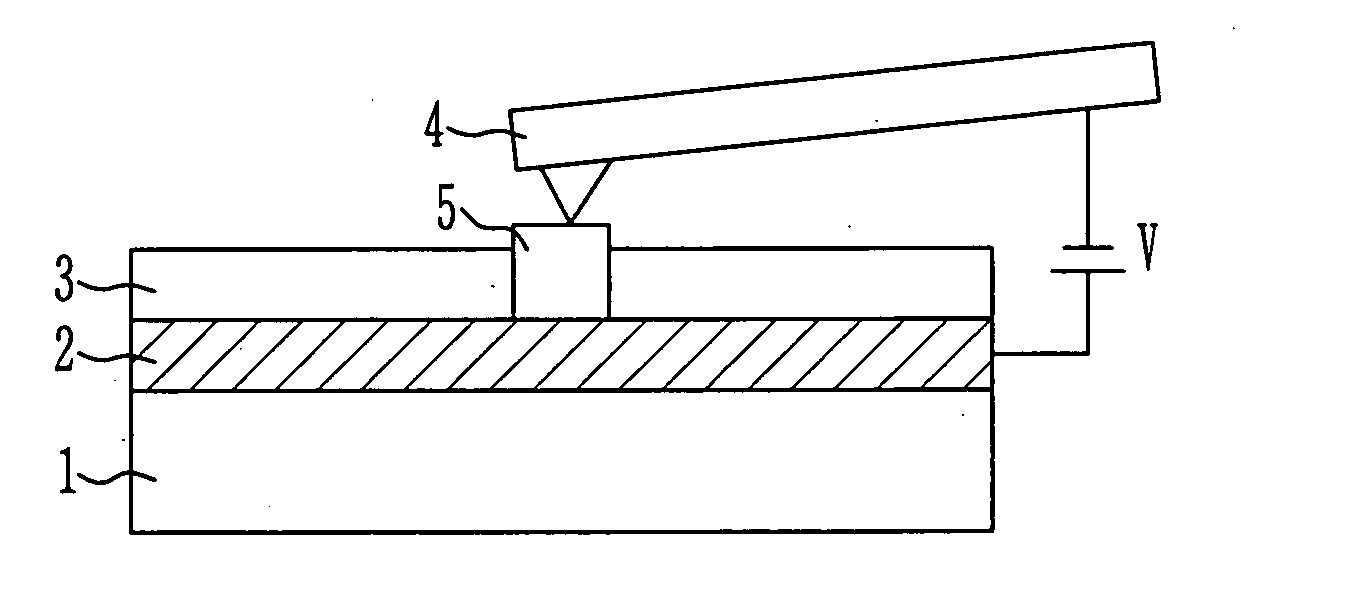
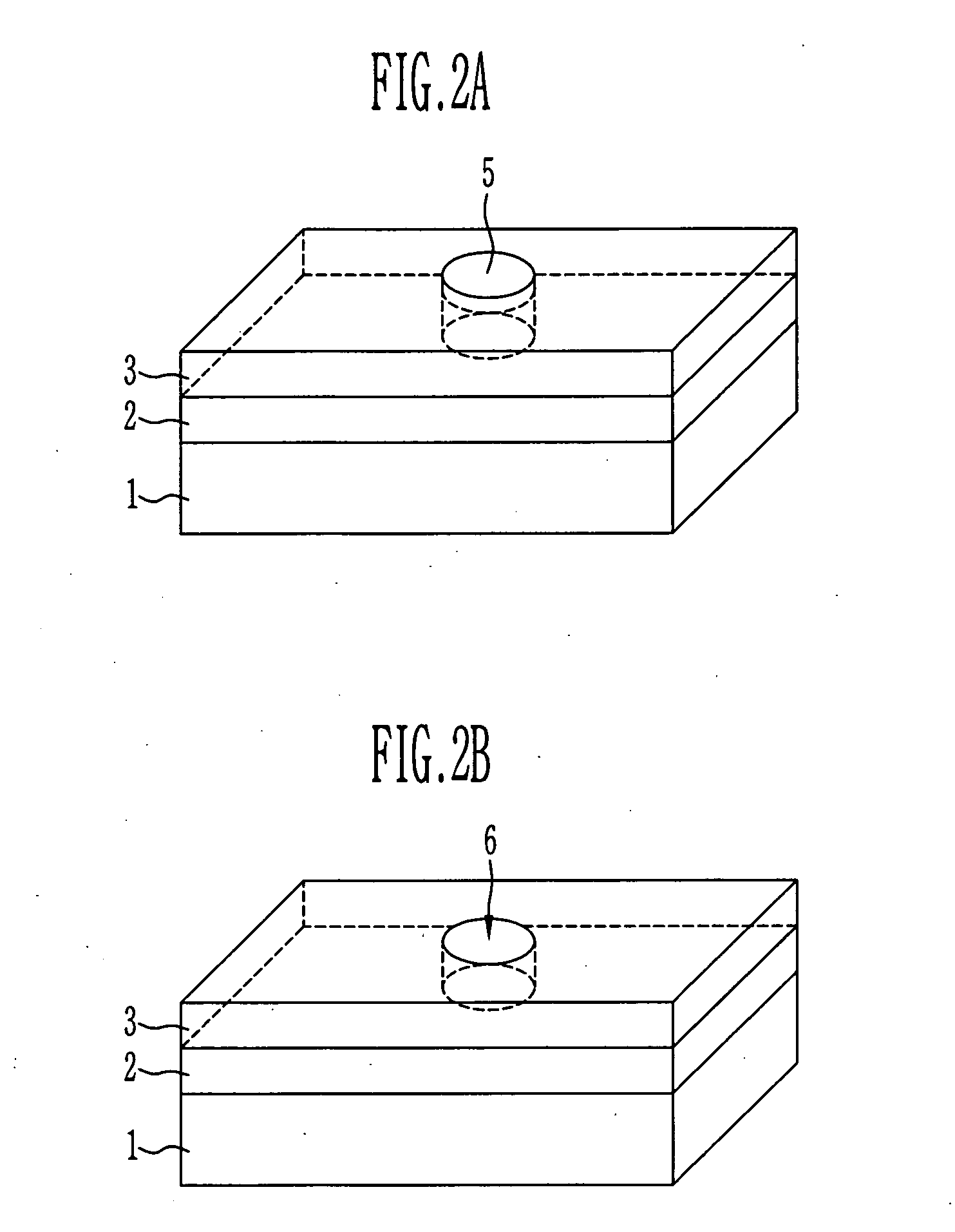
[0011] The present invention is directed to a method for fabricating the nano pore, in which an oxidation pattern is selectively fabricated on a thin mask layer by anodic nano-oxidation using an AFM, so that the nano pore can be fabricated without relatively complicated processes and relatively expensive equipment.

Problems solved by technology

However, the conventional nanoscale structure is fabricated by an electron-beam lithography process, a reactive ion etching (RIE) process, a micro-electromechanical system (MEMS) process, etc., so that its fabrication method is relatively complicated and requires relatively expensive equipment.
As described above, the conventional methods for fabricating the nanoscale pore, using the electron-beam lithography process, the RIE process, the MEMS process, etc., are relatively complicated and require relatively expensive equipment.

Method used


Image

  • Method for fabricating nano pore
  • Method for fabricating nano pore
  • Method for fabricating nano pore

Examples


Embodiment Construction

[0022] Hereinafter, the exemplary embodiments of the present invention will now be described in more detail with reference to the accompanying drawings.

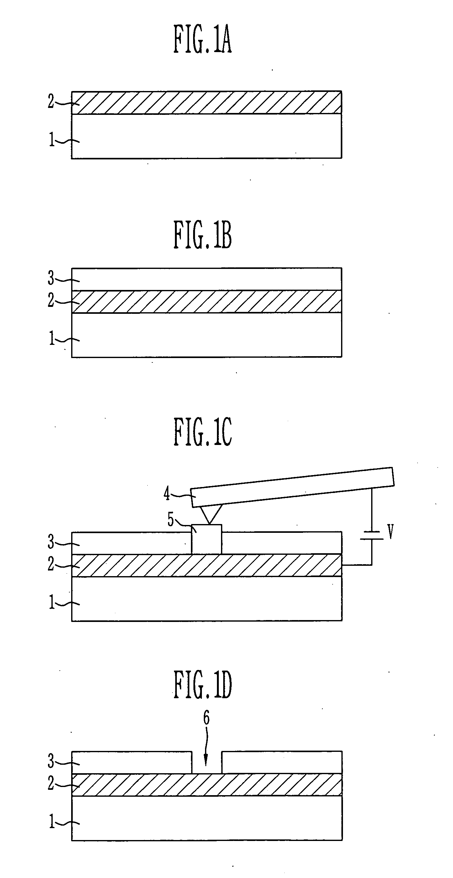
[0023]FIGS. 1A through 1D are cross sectional views for illustrating a process of fabricating a nano pore.

[0024] Referring to FIG. 1A, a bottom layer 2 is formed on a plate 1. Here, the bottom layer 2 is preferably made of silicon dioxide (SiO2), silicon (Si), platinum (Pt), titanium (Ti), chromium (Cr), aluminum (Al), gold (Au), silver (Ag), indium tin oxide (ITO), etc., which are high etching selectivity relative to a thin mask layer to be formed on the bottom layer 2, are capable of forming a self-assembled monolayer, and are easy to adhere molecules thereto.

[0025] Referring to FIG. 1B, the thin mask layer 3 is formed on the bottom layer 2, having a thickness of 1 nm through 30 nm. Here, the thin mask layer 3 is preferably made of silicon (Si), gallium arsenide (GaAs), titanium (Ti), zirconium (Zr), aluminum (Al), chromium (Cr)...


PUM

PropertyMeasurementUnit
thicknessaaaaaaaaaa
thicknessaaaaaaaaaa
bias voltageaaaaaaaaaa

Abstract

Provided is a method for fabricating a nanoscale pore which has been researched in a molecular electronics field of chemistry and in a molecular dynamics field of biology, wherein a oxidation pattern is selectively formed on a thin mask layer by anodic nano-oxidation using an AFM, and the oxidation pattern is selectively etched, thereby fabricating the nanoscale pore. Thus, the present invention provides a simple and easy method for fabricating nano pore array.

Description

BACKGROUND [0001] 1. Field of the Invention [0002] The present invention generally relates to a method for fabricating a nanoscale pore which has been researched in a molecular electronics field of chemistry and in a molecular dynamics field of biology, and more particularly, to a method for fabricating a nano pore using an atomic force microscope (AFM). [0003] 2. Discussion of Related Art [0004] A nanoscale structure has been researched to fabricate a nano electronic device or a single molecule spectroscopy of a biological field. However, the conventional nanoscale structure is fabricated by an electron-beam lithography process, a reactive ion etching (RIE) process, a micro-electromechanical system (MEMS) process, etc., so that its fabrication method is relatively complicated and requires relatively expensive equipment. [0005] As a conventional method related to fabrication of the nano pore structure using the electron-beam lithography process or to nano patterning using nano oxida...

Claims


Application Information

Patent Timeline
Patent Type & Authority Applications(United States)
IPC IPC(8): B05D3/00B05D7/00G03F7/00C25D11/02
CPCB82Y10/00C25D11/022G01Q80/00B82Y30/00G03F7/00B82B3/00B82B1/00
Inventor KIM, JUN HOPARK, KANG HOSONG, KI BONGKIM, EUN KYOUNGLEE, SUNG Q.
Owner ELECTRONICS & TELECOMM RES INST
Learn More