Processing device and processing method

Inactive Publication Date: 2005-07-07
TOKYO ELECTRON LTD
View PDF3 Cites 40 Cited by
  • Summary
  • Abstract
  • Description
  • Claims
  • Application Information

AI Technical Summary

Benefits of technology

[0014] In view of the above situations, the present invention aims at providing a processing device and processing method which acquire pred

Problems solved by technology

Such a vapor phase reaction degrades the quality of a film formed on the substrate.
Therefore, a sufficiently high measuring sensitivity cannot be acquired, and the measured value varies depending on the detection position so that highly reliable information may not be obtained.
In such a case, the reliability of the process falls, such as reduction in film quality, particularly, in ALD that forms a precise film of an atomic layer level.
In this case, as the exhaust pipe has a relatively large diameter, a variation in the distribution of particles in the exhaust pipe becomes larger, disab

Method used


Image

  • Processing device and processing method
  • Processing device and processing method
  • Processing device and processing method

Examples


first embodiment

[0068] (First Embodiment)

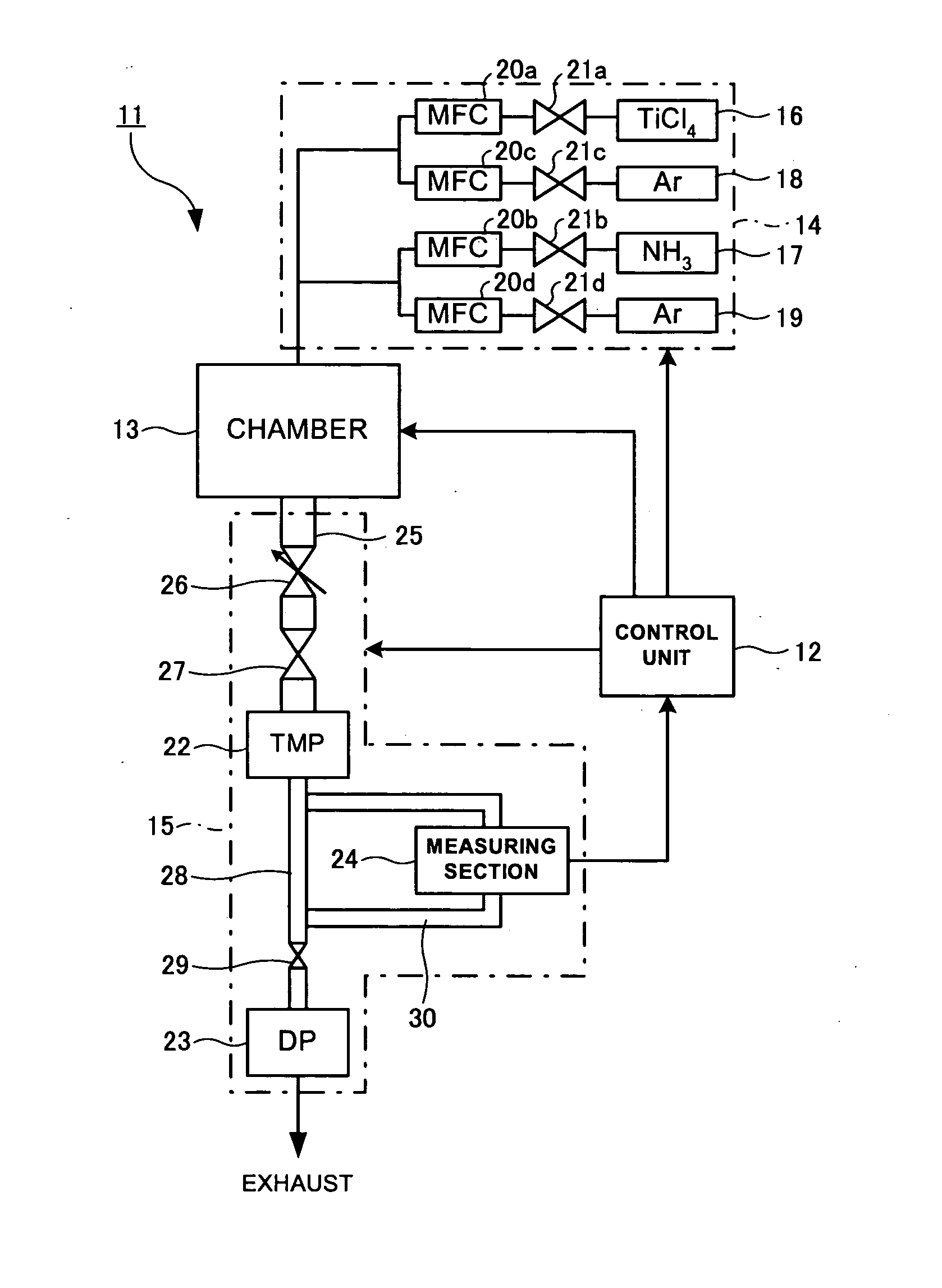
[0069] In the first embodiment, a process system which alternately supplies titanium tetrachloride (TiCl4) gas and ammonia (NH3) gas into the chamber with vacuum exhaust in between and deposits a titanium nitride (TiN) film on the top surface of a semiconductor wafer (hereinafter wafer) using so-called atomic layer deposition (Atomic Layer Deposition; ALD) is described as an example.

[0070]FIG. 1 shows the structure of a process system 11 according to the embodiment.

[0071] As shown in FIG. 1, the process system 11 has a control unit 12, a chamber 13, a gas supply line 14 and an exhaust line 15.

[0072] The control unit 12 controls the general operation of the process system 11 concerning deposition to be discussed later. To make understanding easier, the details of the operation of the control unit 12 are omitted.

[0073] The chamber 13 is constructed in such a way as to be vacuumable and a wafer as a process target is retained therein. An ALD process to be d...

second embodiment

[0113] (Second Embodiment)

[0114] In the second embodiment, dry cleaning of a process system which deposits a silicon-based film of silicon oxide or so, on the top surface of a process target like a semiconductor wafer (hereinafter wafer) by a plasma process in a chamber is described as an example. Dry cleaning of the process system is carried out by introducing the plasma of a fluorine-based gas (nitrogen trifluoride (NF3)) into the chamber.

[0115]FIG. 5 shows the structure of a process system 11 according to the second embodiment. As shown in FIG. 5, the process system 11 has a control unit 12, a chamber 13, a cleaning gas supply line 50 and an exhaust line 15.

[0116] The control unit 12 controls the general operation of the process system 11, such as film deposition and cleaning, to be discussed later. To make understanding easier, the details of the operation of the control unit 12 are omitted.

[0117] The chamber 13 is constructed in such a way as to be vacuumable and a wafer as ...


PUM

PropertyMeasurementUnit
Partial pressureaaaaaaaaaa
Pressureaaaaaaaaaa
Diameteraaaaaaaaaa

Abstract

An exhaust line (15) connected to a chamber (13) comprises a TMP (22) and a dry pump (23). The chamber (13) and the TMP (22) are connected by a first exhaust pipe (25), and the TMP (22) and the dry pump (23) are connected by a second exhaust pipe (28). A measuring section (24) monitors a partial pressure of TiCl4 or NH3 in an exhaust gas flowing in the second exhaust pipe (28). Two types of process gases are alternately supplied into the chamber (13) for a predetermined time, and when the partial pressure of one of the supplied process gases in the exhaust gas is reduced to a predetermined value, a control means (12) starts supplying the other process gas.

Description

TECHNICAL FIELD [0001] The present invention relates to a processing device and processing method which perform a predetermined process, such as deposition, on a process target such as a semiconductor wafer. BACKGROUND ART [0002] At present, micronization and large scale integration of semiconductor integrated circuits advance miniaturization of patterns, such as wiring grooves formed in the substrate surface of a substrate or the like. In case where a thin film is formed as an underlayer of wiring metal, therefore, it is demanded to form a very thin film in a fine patterned wiring groove uniformly with a good coverage. In accordance with this demand, a method called atomic layer deposition (Atomic Layer Deposition; ALD) has recently been developed as a method capable of forming a good-quality film of an atomic layer level. [0003] ALD comprises the following steps, for example. In the example illustrated below, a description is given of a case where an underlayer of titanium nitride...

Claims


Application Information

Patent Timeline
IPC IPC(8): C23C16/44C23C16/455C23C16/52H01L21/285H01L21/3065H01L21/31H01L21/768
CPCC23C16/4412C23C16/45525H01L21/76843H01L21/28562C23C16/52
Inventor KANNAN, HIROSHIMATSUOKA, TAKAAKI
Owner TOKYO ELECTRON LTD
Why Eureka
Try Eureka