Low profile active electronically scanned antenna (AESA) for ka-band radar systems

a radar system and low-profile technology, applied in the field of radar and communication systems, can solve problems such as heat extraction from high-power electronic devices, and experience what appears to be insurmountable difficulties

Inactive Publication Date: 2005-07-07
NORTHROP GRUMMAN SYST CORP
View PDF27 Cites 55 Cited by
  • Summary
  • Abstract
  • Description
  • Claims
  • Application Information

AI Technical Summary

Benefits of technology

[0009] These and other objects are achieved by an architecture for a Ka-band multi-function radar system (KAMS) comprised of multiple parallel layers of electronics circuitry and waveguide components which are stacked together so as to form a unitary structure behind an antenna faceplate. The invention includes the concepts of vertical integration and solderless interconnects of active electronic circuits while maintaining the required array grid spacing for Ka-band operation and comprises, among other things, a transitioning RF waveguide relocator panel located behind a radiator faceplate and an array of beam control tiles respectively coupled to one of a plurality of transceiver modules via an RF manifold. Each of the beam control tiles includes respective high power transmit/receive (T/R) cells as well as RF stripline and coaxial transmission line elements. In the preferred embodiment of the invention, the waveguide relocator panel is comprised of a diffusion bonded copper laminate stack up with dielectric filling while the beam control ti...

Problems solved by technology

Accordingly, previous attempts to design low profile electronically scanned antenna arrays for ground and air vehicles and operating at Ka-band have experienced what appears to be insurmountable difficulties be...

Method used


Image

  • Low profile active electronically scanned antenna (AESA) for ka-band radar systems
  • Low profile active electronically scanned antenna (AESA) for ka-band radar systems
  • Low profile active electronically scanned antenna (AESA) for ka-band radar systems

Examples


Embodiment Construction

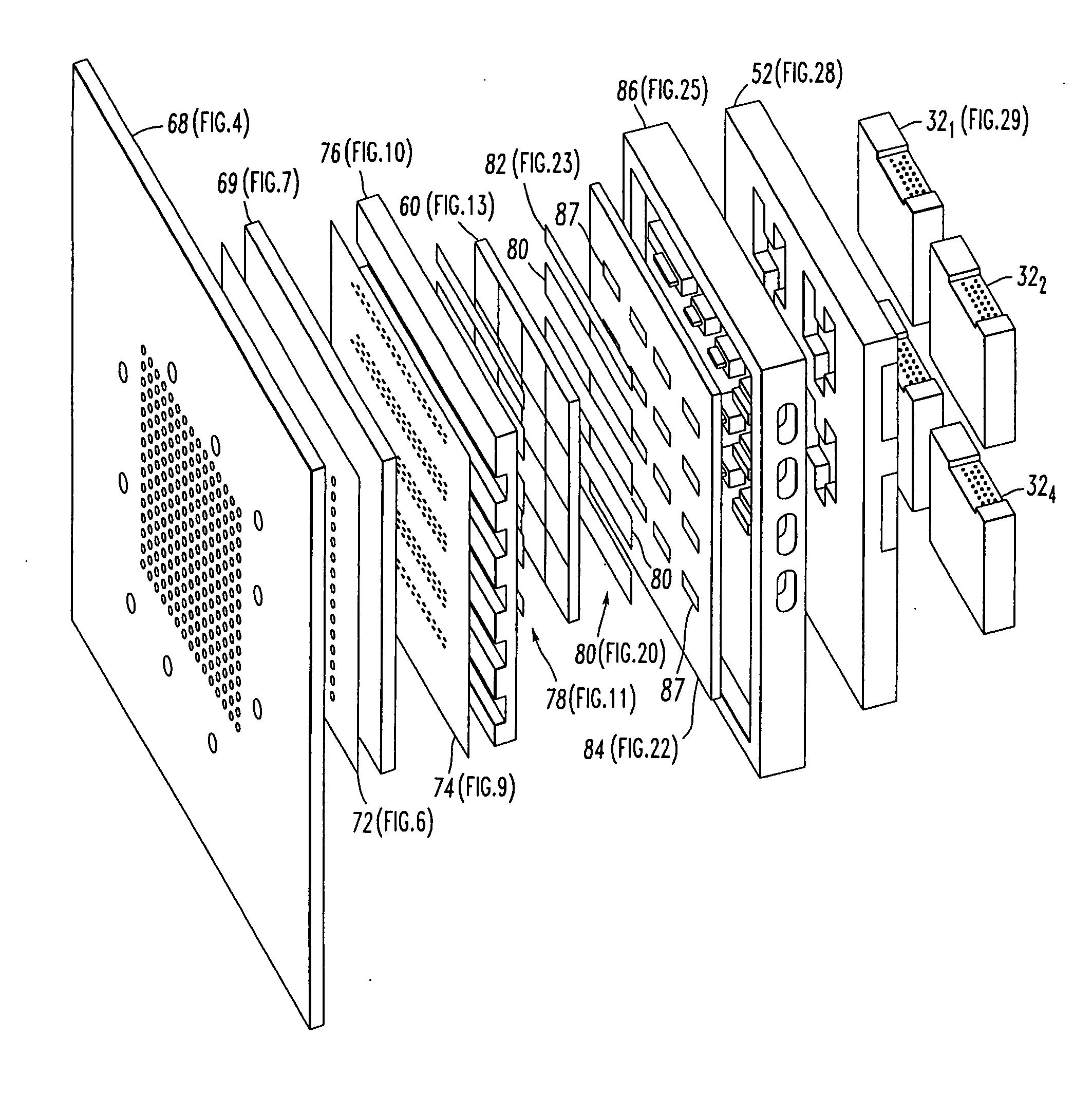
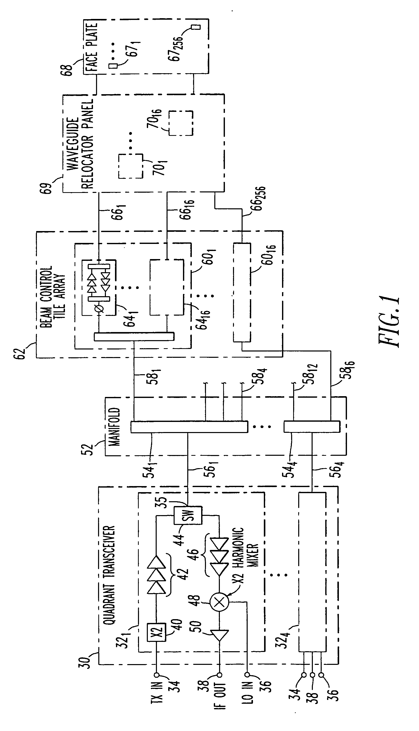
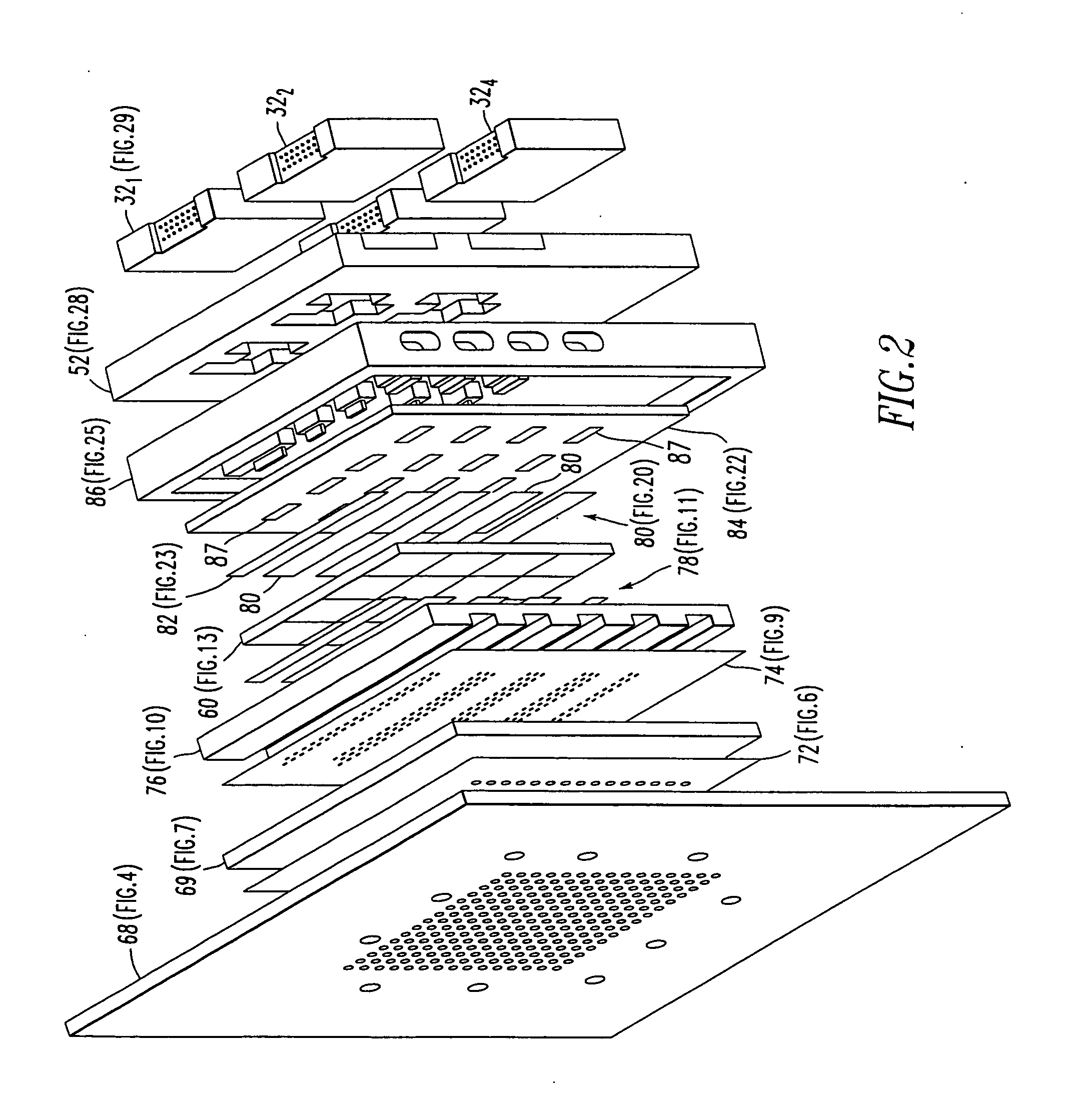
[0042] Referring now to the various drawing figures wherein like reference numerals refer to like components throughout, reference is first made to FIG. 1 wherein there is shown an electrical block diagram broadly illustrative of the subject invention and which is directed to a Ka-band multi-function system (KAMS) active bidirectional electronically scanned antenna (AESA) array utilized for both transmitting and receiving RF signals to and from a target.

[0043] In FIG. 1, reference numeral 30 denotes a transceiver module sub-assembly comprised of four transceiver modules 321 . . . 324, each including an input terminal 34 for RF signals to be transmitted, a local oscillator input terminal 36 and a receive IF output terminal 38. Each transceiver module, for example module 321, also includes a frequency doubler 40, transmit RF amplifier circuitry 42, and a transmit / receive (T / R) switch 44. Also included is receive RF amplifier circuitry 46 coupled to the T / R switch 44. The receive ampl...


PUM


Abstract

A vertically integrated Ka-band active electronically scanned antenna including, among other things, a transitioning RF waveguide relocator panel located behind a radiator faceplate and an array of beam control tiles respectively coupled to one of a plurality of transceiver modules via an RF manifold. Each of the beam control tiles includes a respective plurality of high power transmit/receive (T/R) cells as well as dielectric waveguides, RF stripline and coaxial transmission line elements. The waveguide relocator panel is preferably fabricated by a diffusion bonded copper laminate stack up with dielectric filling. The beam control tiles are preferably fabricated by the use of multiple layers of low temperature co-fired ceramic (LTCC) material laminated together. The waveguide relocator panel and the beam control tiles are designed to route RF signals to and from a respective transceiver module of four transceiver modules and a quadrature array of antenna radiators matched to free space formed in the faceplate. Planar type metal spring gaskets are provided between the interfacing layers so as to provide and ensure interconnection between mutually facing waveguide ports and to prevent RF leakage from around the perimeter of the waveguide ports. Cooling of the various components is achieved by a pair of planar forced air heat sink members which are located on either side of the array of beam control tiles. DC power and control of the T/R cells is provided by a printed circuit wiring board assembly located adjacent to the array of beam controlled tiles with solderless DC connections being provided by an arrangement of “fuzz button” electrical connector elements.

Description

CROSS REFERENCE TO RELATED APPLICATION [0001] This application is a Division of application Ser. No. 10 / 358,278, entitled “Low Profile Active Electronically Scanned Antenna (AESA) for Ka-Band Radar Systems”, filed in the United States Patent and Trademark Office on Feb. 5, 2003, and assigned to the assignee of the present application.BACKGROUND OF THE INVENTION [0002] This invention relates generally to radar and communication systems and more particularly to an active phased array radar system operating in the Ka-band above 30 GHz. [0003] Active electronically scanned antenna (AESA) arrays are generally well known. Such apparatus typically requires amplifier and phase shifter electronics that are spaced every half wavelength in a two dimensional array. Known prior art AESA systems have been developed at 10 GHz and below, and in such systems, array element spacing is greater than 0.8 inches and provides sufficient area for the array electronics to be laid out on a single circuit lay...

Claims


Application Information

Patent Timeline
IPC IPC(8): H01P1/04H01P1/26H01P5/08H01P5/107H01Q1/42H01Q3/26H01Q21/00H01Q21/06H01Q23/00
CPCH01P1/047H01P1/268H01P5/085H01P5/107H01Q23/00H01Q3/26H01Q21/0037H01Q21/0087H01Q21/064H01Q1/422
Inventor STENGER, PETER A.KUSS, FRED C.LACOUR, KEVINHEFFNER, CRAIGSISK, ROBERTWISE, CARL D.PAQUIN, JOSEPHHINTON, TUJUANAWALTERS, ANDREWKRAFCSIK, DAVIDMCMONAGLE, BRIAN T.BLOCK, STEVEN D.HANDLEY, STEVEN S.
Owner NORTHROP GRUMMAN SYST CORP
Why Eureka
Try Eureka