Semiconductor integrated circuit, liquid crystal drive device, and liquid crystal display system

a technology of integrated circuits and liquid crystal drives, applied in the direction of electric digital data processing, instruments, computing, etc., can solve the problem that the fluctuation permissible width of the center voltage of the input differential signals yp and yn cannot be also widened, and the output voltage of the differential amplification stage cannot be easily adjusted. problem, to achieve the effect of easy adjustmen

Inactive Publication Date: 2005-07-07
RENESAS ELECTRONICS CORP +1
View PDF5 Cites 30 Cited by
  • Summary
  • Abstract
  • Description
  • Claims
  • Application Information

AI Technical Summary

Benefits of technology

[0029] With such a configuration, even when conditions such as manufacture variations of semiconductors, the center voltage of differential external clocks, power supply voltage, temperature and the like chang

Problems solved by technology

As understood also from Equation (1), if the gate-source voltage Vgs decreases, a problem such that when the threshold voltage Vth is deviated from a reference value due to variation in process of the MOSFET, the variation exerts a large influence on the current value I and a problem such that a gate width has to be increased to pass the same current occur.
It causes a problem such that the fluctuation permissible width of the center voltage of the input differential signals YP and YN cannot be also widened.
Further, when the potential of the common source of the differential input MOSFETs Q62 and Q63

Method used


Image

  • Semiconductor integrated circuit, liquid crystal drive device, and liquid crystal display system
  • Semiconductor integrated circuit, liquid crystal drive device, and liquid crystal display system
  • Semiconductor integrated circuit, liquid crystal drive device, and liquid crystal display system

Examples


first embodiment

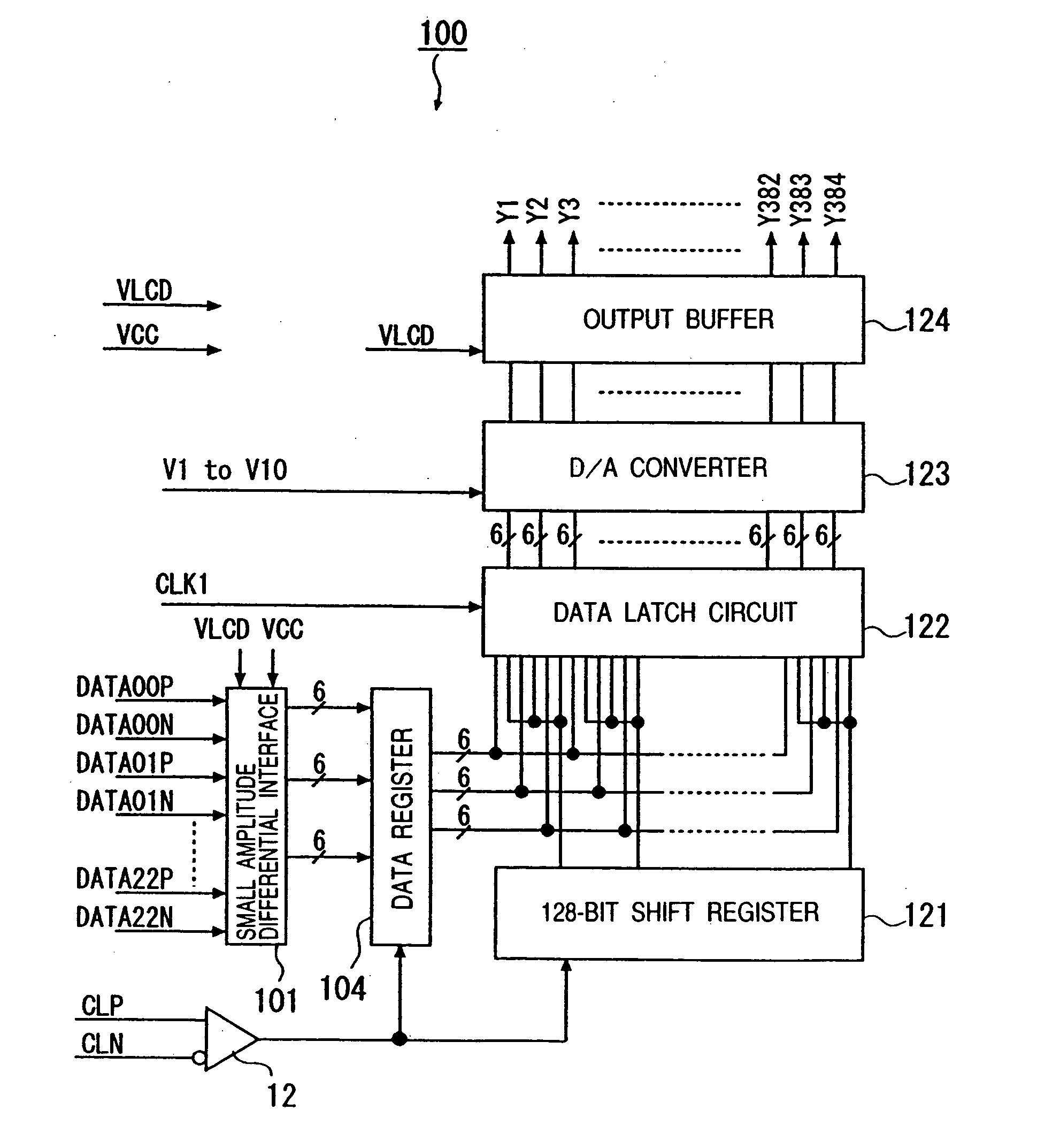
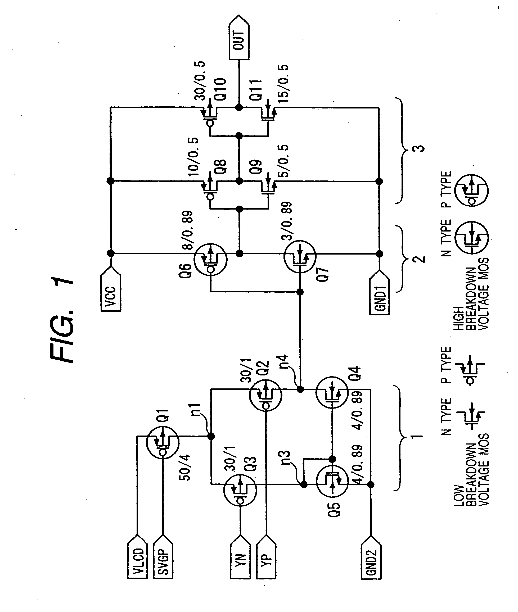
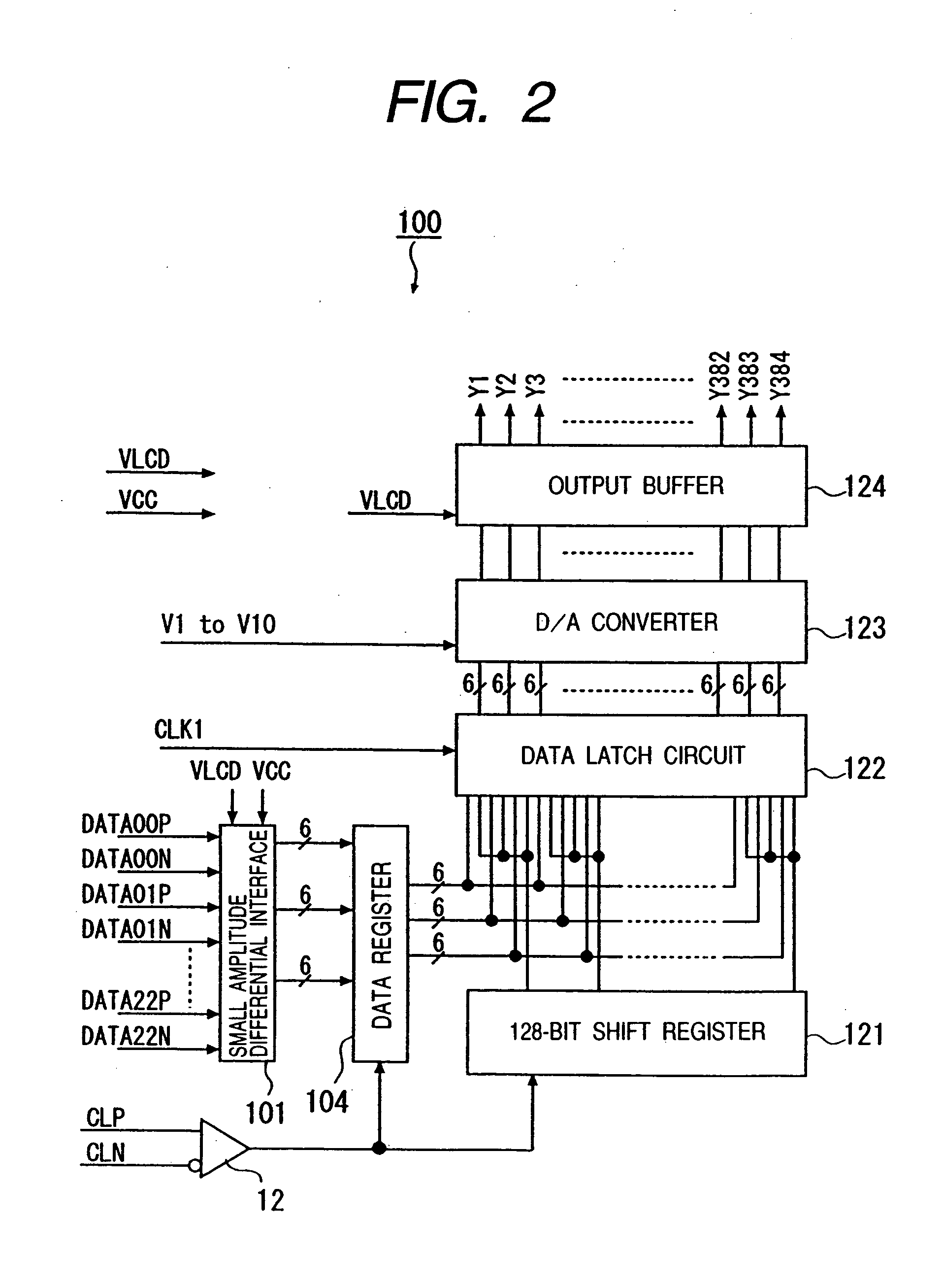
[0053]FIG. 1 is a circuit diagram specifically showing an example of a small amplitude differential signal interface to which the invention is suitably applied. In the diagram, beside each MOSFET, the ratio “W / L” of gate width W(μm) and gate length L (μm) as an example of a preferable numerical value is shown.

[0054] A small amplitude difference signal interface (differential input circuit) of the embodiment is an LVDS (Low Voltage Differential Signaling) interface or a small amplitude differential signal interface as a derivative technique of the LVDS interface specified in IEEE (Institute of Electrical and Electronics Engineers) . For example, the interface receives a small amplitude differential signal (having an amplitude of 200 mV to 500 mV) input from the outside such as an external clock and a data signal and outputs a high-level or low-level signal to an internal circuit in accordance with a voltage difference between a pair of small amplitude differential signals.

[0055] As...

second embodiment

[0104] In a second embodiment, a standby function for interrupting, when unnecessary, the operation current of the differential amplification stage 1 in the small amplitude differential signal interface 101 to which the differential display data DATAP and DATAN is input is added to the liquid crystal driver 100 described in the first embodiment. Specifically, the power supply voltages (VLCD, VDD2) of the differential amplification stage 1 in the small amplitude differential signal interface 101 described in the first embodiment are set to be higher than the power supply voltage (VCC) of the internal circuits, so that the consumption power of the differential amplification stage 1 becomes an unignorable value. Since the liquid crystal system is constructed by using, for example, eight liquid crystal drivers 100 of the first embodiment, it is considered that the power consumption of the system is high. In the second embodiment, therefore, the liquid crystal driver 100 capable of reduc...

third embodiment

[0134]FIG. 21 is a circuit diagram showing an input section of display data and transfer clocks in a liquid crystal driver of a third embodiment.

[0135] In the third embodiment, in the liquid crystal driver shown in the first and second embodiments, an input circuit of the transfer clock CL2 for giving the transfer timing of the display data DATA is improved.

[0136] In the case of receiving differential transfer clocks CL2 (the positive phase side of the clock is indicated as CL2P and the negative phase side of the clock is indicated as CL2N) by a differential amplifier, it is difficult to set the rising time and the falling time of the transfer clock CL2 passing through the differential amplification stage to the same due to characteristics of the differential amplifier. A deviation occurs between the rising time and the falling time according to the conditions such as the center voltage of the differential signals, power supply voltage, and temperature. Therefore, in the transfer ...


PUM


Abstract

A liquid crystal drive device having a differential-type input circuit including a differential amplification stage for receiving a differential signal and a buffer stage for generating an output signal on the basis of an output of the differential amplification stage, the liquid crystal drive device for receiving a signal of display data via the input circuit and outputting a signal for driving a liquid crystal panel on the basis of the display data, wherein a liquid crystal driving voltage VLCD larger than a power supply voltage VCC for logic to be supplied to the operation voltage buffer stage is supplied to the differential amplification stage of the input circuit. A standby function of interrupting an operation current of the differential amplification stage in a period where no display data is received is provided.

Description

TECHNICAL FIELD [0001] The present invention relates to a technique useful for application to a semiconductor integrated circuit having a differential circuit such as a small amplitude differential signal interface and, further, a technique which is particularly useful for a semiconductor integrated circuit for receiving two kinds of power supplies such as a liquid crystal driver. BACKGROUND ART [0002] Liquid crystal drivers for driving a data line of a TFT (Thin Film Transistor) liquid crystal panel used as a display in a notebook-sized computer or the like include a liquid crystal driver for receiving digital display data of 6 bits per pixel at high speed and generating 384 liquid crystal driving output voltages in 64 tones on the basis of the digital data. In recent years, as a interface for transmitting / receiving digital data at high speed in such a liquid crystal driver, an LVDS (Low Voltage Differential Signaling) interface or a small amplitude differential signal interface as...

Claims


Application Information

Patent Timeline
IPC IPC(8): G09G3/36
CPCG09G3/3611G09G3/3688G09G3/3696G09G2310/027G09G2310/0297G09G2370/08G09G2330/021G09G2330/022G09G2330/06G09G2360/02G09G2330/02G09G3/36
Inventor KINJO, ARATAOOKADO, KAZUOKOTERA, KOUICHIODA, HITOSHIENDO, MASUHIRO
Owner RENESAS ELECTRONICS CORP
Why Eureka
Try Eureka