

Non-volatile memory array having vertical transistors and manufacturing method thereof
- Summary
- Abstract
- Description
- Claims
- Application Information
AI Technical Summary
Benefits of technology
Problems solved by technology
Method used
Image

Examples
Embodiment Construction
[0025] Embodiments of the present invention are now being described, with reference to the accompanying drawings.
[0026] A process for making a memory array having vertical transistors of NMOS type is exemplified as follows, with a view to illustrating the features of the present invention.
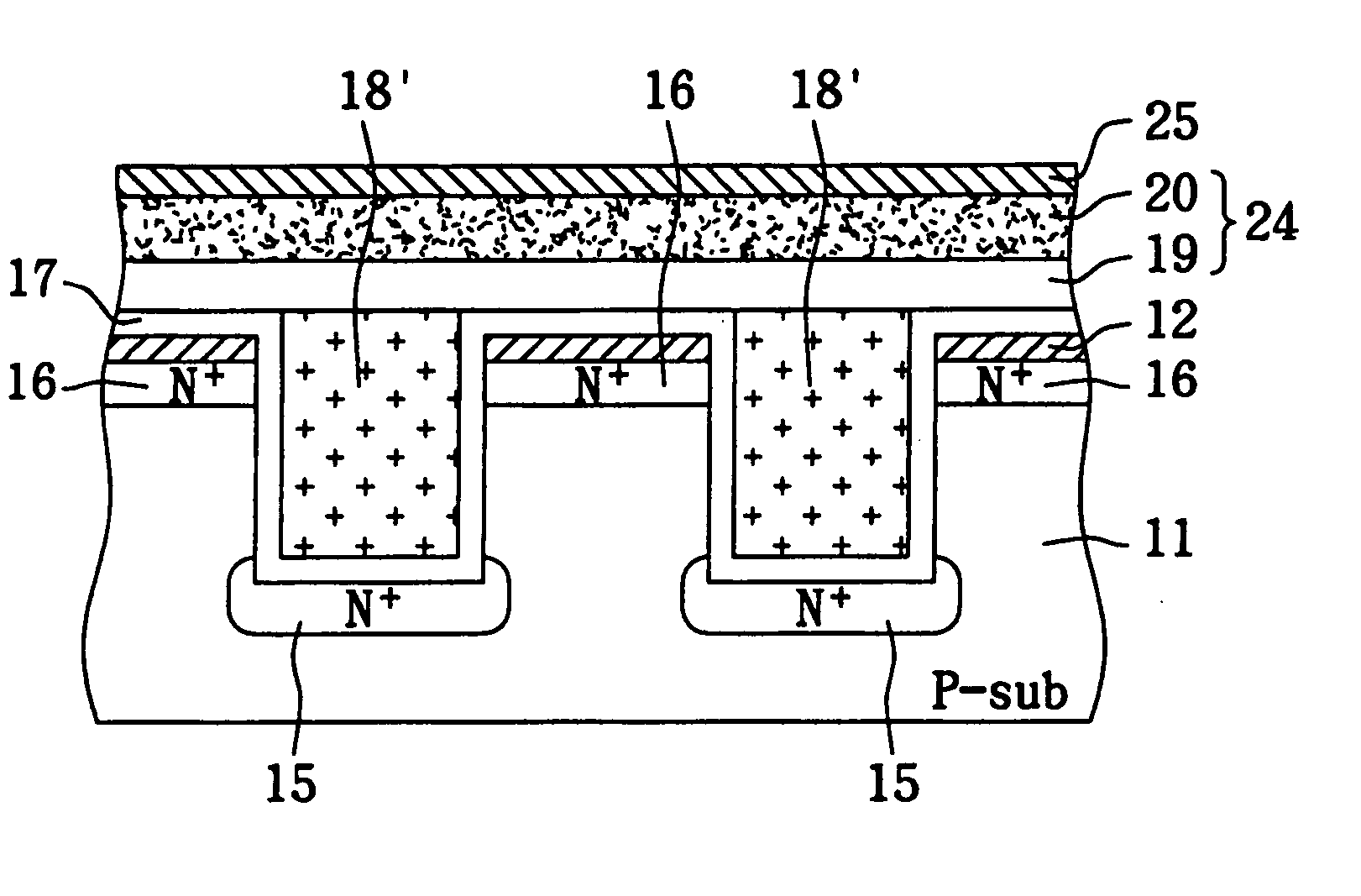
[0027]FIGS. 2 through 10 illustrate the memory structures at each step of the manufacturing process of a non-volatile memory array having vertical transistors in accordance with the present invention. In FIG. 2, a mask layer 12 is formed on a surface of a semiconductor substrate 11, e.g., a silicon substrate, where the mask layer 12 is typical of a thickness between 100-2000 angstroms, and can be composed of silicon nitride (SixNy), silicon oxide (SiOx), silicon oxynitride (SiOxNy) or multi-layer of the films. Then, a photoresist layer 13 is deposited on the surface of the mask layer 12, and is patterned to define multiple trenches as shown in FIG. 3. In FIG. 4, the mask layer 12 and the semicond...
PUM
 Abstract
Description
Claims
Application Information