

Electrolytic processing apparatus and electrolytic processing method
- Summary
- Abstract
- Description
- Claims
- Application Information
AI Technical Summary
Benefits of technology
Problems solved by technology
Method used
Image

Examples
Embodiment Construction
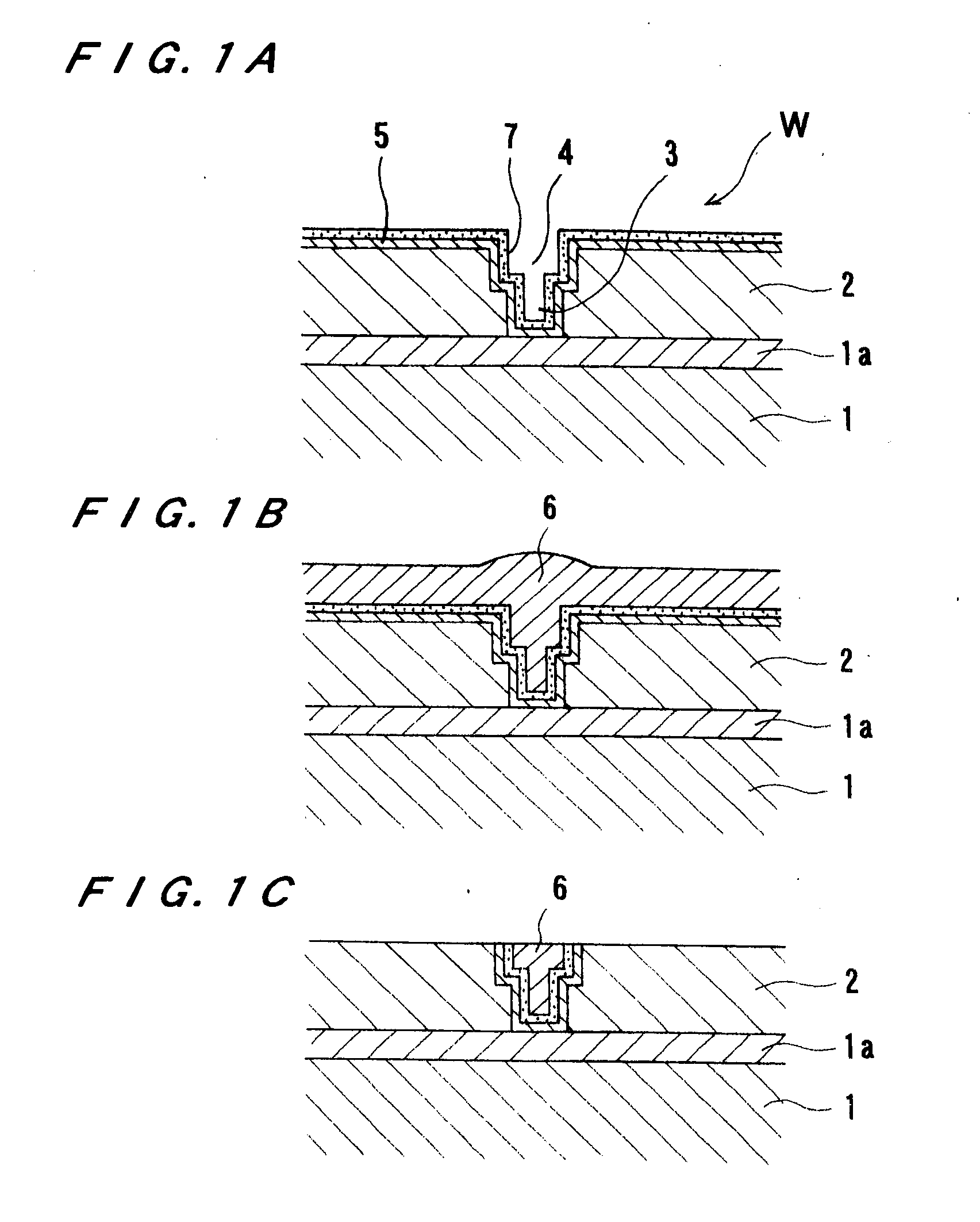
[0087] Preferred embodiments of the present invention will now be described in detail with reference to the drawings. Though the following description illustrates the case of removing a thin film (conductive film), such as a copper film, formed on a surface of a substrate as a workpiece, the present invention is of course applicable to workpieces other than a substrate.
[0088]FIG. 3 is a plan view illustrating the construction of a substrate processing apparatus incorporated an electrolytic processing apparatus according to an embodiment of the present invention. As shown in FIG. 3, the substrate processing apparatus comprises a pair of loading / unloading section 30 as a carry-in / carry-out section for carrying in and out a substrate, e.g. a substrate W having a copper film 6 and a barrier layer as a conductive film (portion to be processed) thereon, as shown in FIG. 1B, a first cleaning machine 31a for performing a primary cleaning of the substrate, a second cleaning machine 31b for ...
PUM
| Property | Measurement | Unit |
|---|---|---|
| Length | aaaaa | aaaaa |
| Thickness | aaaaa | aaaaa |
| Electrical conductivity | aaaaa | aaaaa |
Abstract
Description
Claims
Application Information