Noise filter circuit

Inactive Publication Date: 2005-07-21
NANOPOWER SOLUTION
View PDF4 Cites 3 Cited by
  • Summary
  • Abstract
  • Description
  • Claims
  • Application Information

AI Technical Summary

Benefits of technology

[0103] As described above, according to the present invention, the ripple noise rejection rate and the operation stability, far more excellent than in the prior art, can be realized with very low operating current, without raising the amplification degree and separating the location of the pole by a special method.
[0104] The present invention proposes the circuit configuration that does not exist in the prior art and realizes the very effective ripple noise rejection rate by canceling the ripple noise with a small number of components under the condition of very low operating current.

Problems solved by technology

In a cellular phone, among others, the highest ripple cancellation rate is required because a poor ripple cancellation rate in a power supply of a transmitting section degrades the clarity of the voice conversation.
Even in a digitally coded wireless communication means, a carrier signal is modulated and demodulated in an analog manner during the modulation and the demodulation, and therefore the power source ripple noises adversely influence the error rate.
Though some inventions are proposed as described later, there is no proposal that drastically reduces the low operating current and realizes the high ripple cancellation rate.
These properties are inconvenient for the ripple cancellation rate, whereby particularly the ripple cancellation rate in the low band is to be greatly influenced by the source voltage dependency coefficient of the reference voltage.
Therefore, this requires very great costs in a widely used semiconductor manufacturing method.
The ripple noise of Vref contains a very low frequency and a high frequency component, and therefore a large time constant is required for a filter, whereby a filter rejecting all the frequency bands cannot be integrated on the same semiconductor chip.
In case of no load condition, it moves to very low frequency to make a large phase delay, which is likely to cause an unstable state.
Therefore, a capacitor of a certain type may make the operation unstable.
However, in the conventional circuit, this phase compensation degrades the PSRR very much.
Therefore, the phase allowance is reduced and instability may be caused.
At this time, when Fp3 is close to the polar frequency Fp2 and the gain is large, the operation becomes unstable.
However, this measure allows the power ripple noises to pass from pd to Vout, because a capacitor of a few pF−a few 10 pF is added to the gate of P4, so that the ripple noise rejection is unavoidably sacrificed thereby.
Namely, in the conventional circuit, when the operating current is decreased, the phase rotation occurs from the low frequency and the gain is not reduced, so that a stable operation cannot be attained.
However, C3 requires a large capacitance value and therefore the conventional circuit cannot be applied to a small apparatus.
As a result, there is a problem that the PSRR is drastically decreased.
The circuit has a two-stage amplification structure and therefore an insufficient gain results in poor characteristics.
As described above, it is understood that the conventional circuit system cannot attain the excellent rippler ejection rate, unless the operating current is sufficiently large.

Method used


Image

  • Noise filter circuit
  • Noise filter circuit
  • Noise filter circuit

Examples


first embodiment

(First Embodiment)

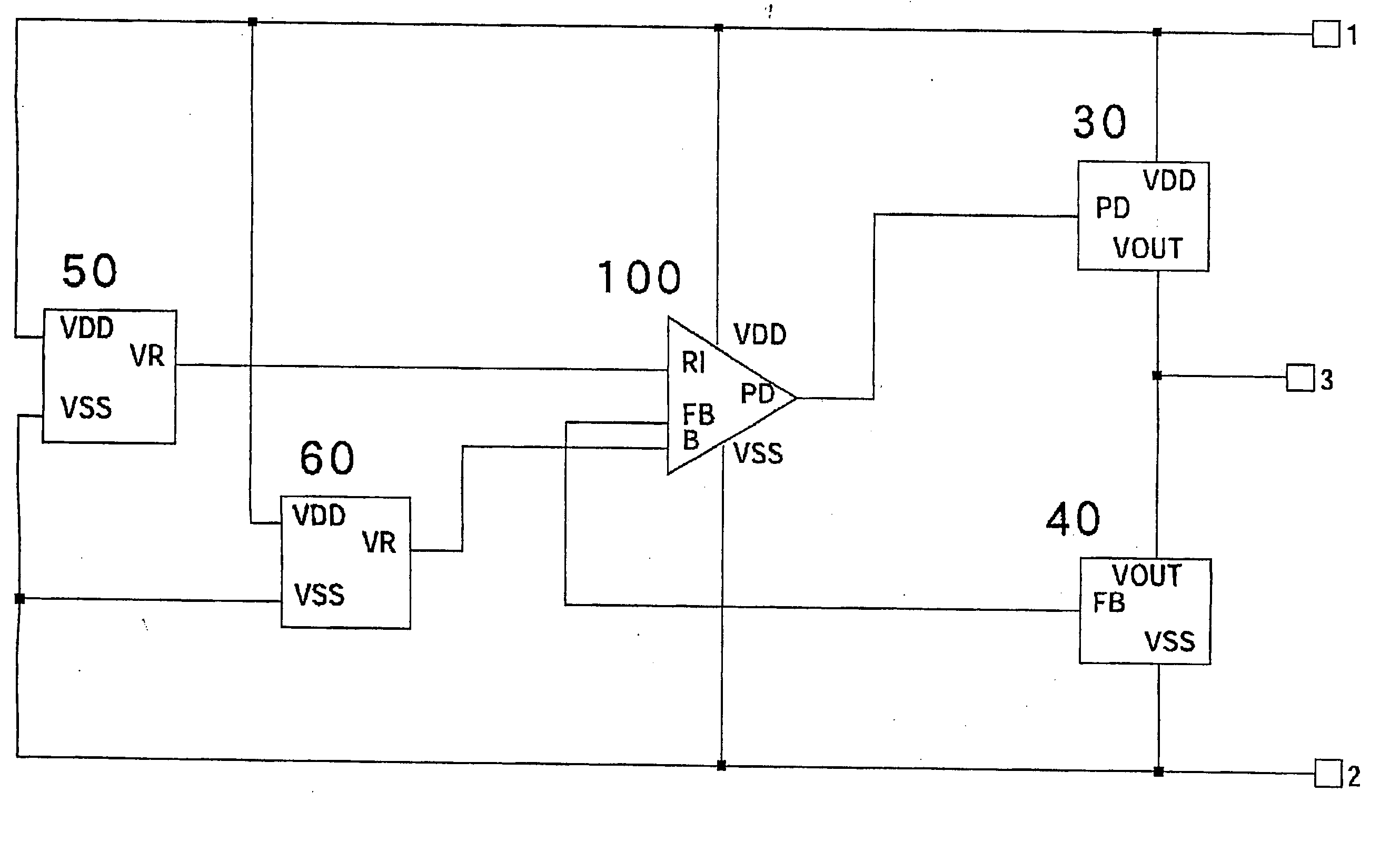
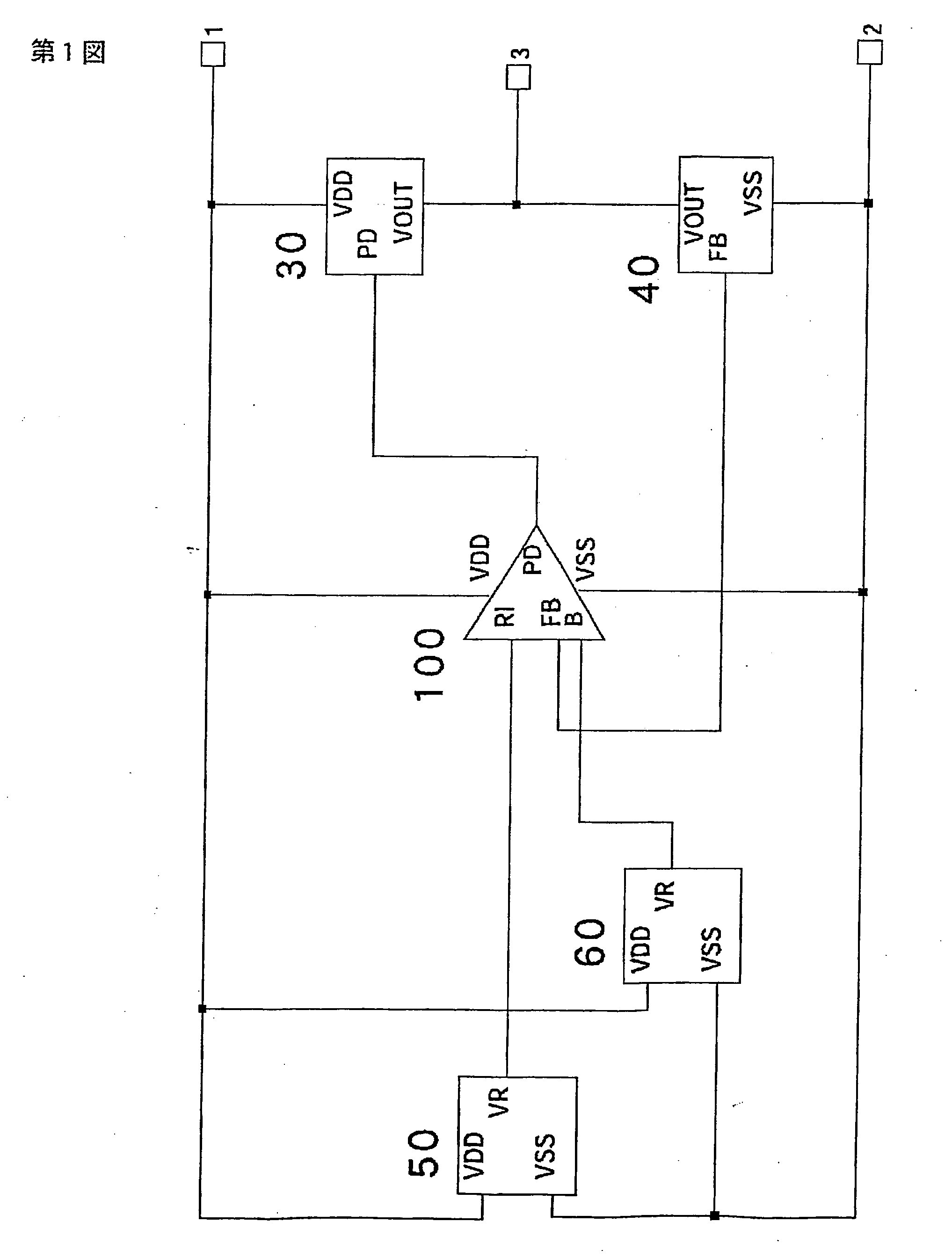
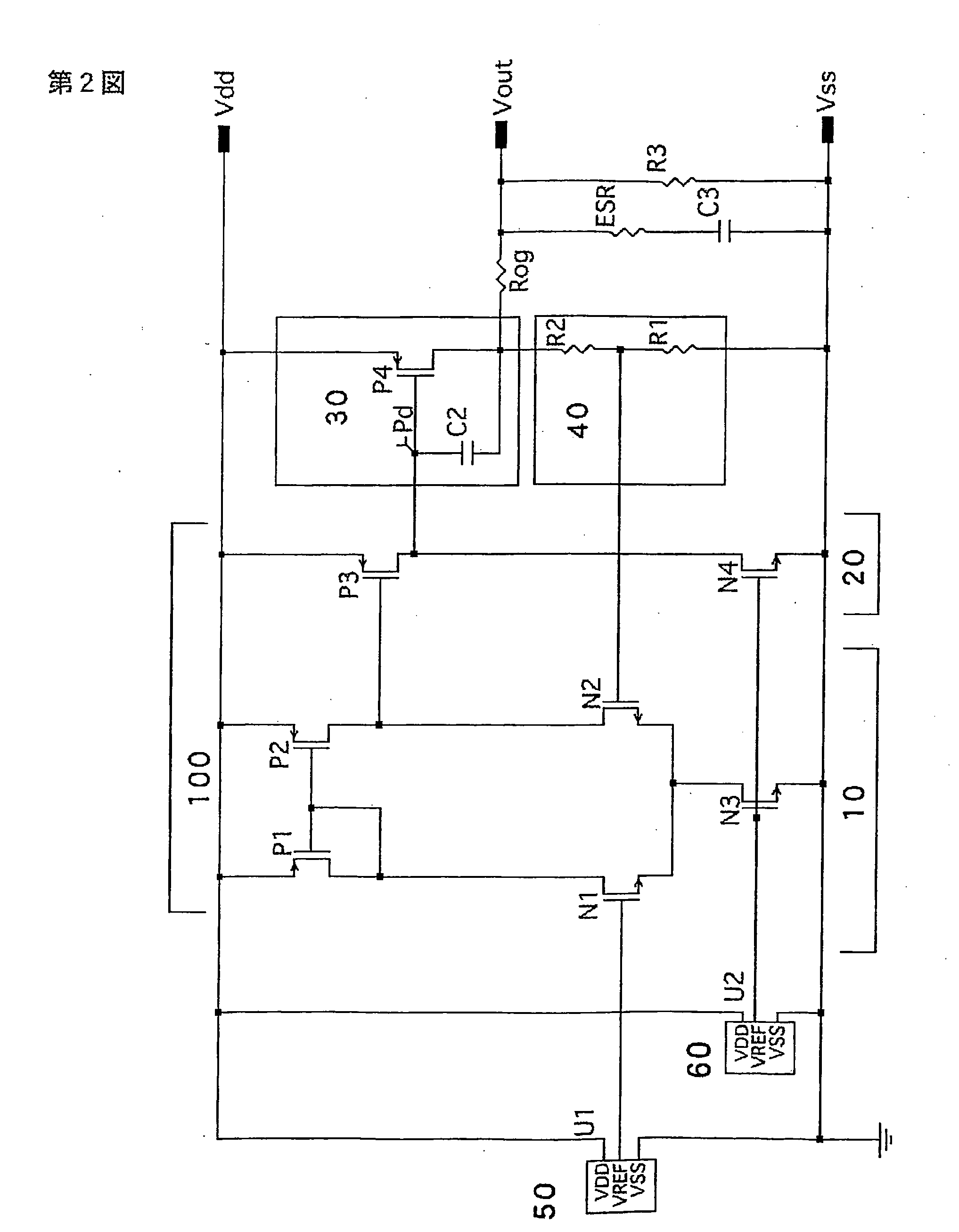
[0064]FIG. 18 is a block diagram showing a first embodiment, and FIG. 7 shows a concrete circuit configuration thereof. In line with the circuit configuration in FIG. 2, stated as prior art, in FIG. 7 the error amplifier 100 is a two-stage amplifier; a differential amplifier 10 as a first stage and a phase inverting amplifier 20 as a second stage. The numerals 30, 40, 50 and 60 indicate an output buffer, an error detection voltage-dividing circuit, a reference voltage circuit and a bias current generation circuit, respectively. The difference from the prior art lies in an additional canceling signal generation circuit 80 connected to the input terminal N2.

[0065] The canceling signal generation circuit 80 generates a very finely divided and advanced-phase signal from a noise signal generated in a power source line, and feeds it to the input of the error amplifier circuit, to reject the ripple noise in the high frequency band. FIG. 8 is a variation of the embodiment...

second embodiment

(Second Embodiment)

[0075] Next, the second embodiment of the present invention will be explained by referring to the block diagram of FIG. 19 and the circuit diagram of FIG. 15. The same constituent elements as those in FIG. 7 are indicated with the same numerals.

[0076] In FIG. 15, in comparison with the first embodiment shown in FIG. 7, the canceling transistor array 70, (N5, N6 and N7) is added. The gate of the canceling transistor array 70 is connected to the power source, and the ripple noise signal on the power source line is directly added.

[0077] The cascade transistors like N5 and N6, included in the canceling transistor array 70, are mentioned in the reference U.S. Pat. No. 4,533,877 that shows the improvement of the PSRR. Another reference U.S. Pat. No. 5,113,148 also exemplifies the cascaded transistors. The gate terminal of all the conventional cascaded transistors is connected to a dedicated reference voltage for matching the current values. Otherwise, a current mismat...

third embodiment

(Third Embodiment)

[0081] A block diagram in FIG. 20 shows a third embodiment of the present invention. The circuit shown in FIG. 16 is its concrete circuit configuration. The same components as those in FIG. 7 are designated by the same symbols. In the present embodiment, both of the canceling signal generation circuit 80 and the canceling transistor array 70 are implemented.

[0082] As a variation of the above-mentioned embodiment, a circuit diagram is shown in FIG. 17. In this circuit configuration, the bias current generation circuit 60 is omitted and the reference voltage generation circuit 50 can also serve as the bias current generation circuit.

(Inclination of System Offset—1)

[0083]FIG. 9 is a graph showing the simulation of the dependency characteristics of each circuit section when the power voltage Vdd changes in the embodiment shown in FIG. 15. The curves 94 and 91 indicate the drain current and the output voltage Vout of P3, respectively in case of absence of the cancel...


PUM


Abstract

A noise canceling circuit, comprising: a first source terminal; a second source terminal; a reference voltage generation means for generating a reference voltage; a bias current generation means for generating a bias current determining an operating current; an error amplifier means for amplifying an error voltage for the reference voltage, the error amplifier means containing at least one phase compensation capacitor; a voltage-current output means for generating an output of a power circuit; and an output voltage-dividing means for detecting a fluctuation of the output voltage, wherein: a first input terminal of the error amplifier means is connected to the reference voltage generation means; a second input terminal of the error amplifier means is connected to the output voltage-dividing means; the error amplifier means comprises an input part consisting of a pair of the 1-type semiconductor elements and a load part consisting of a pair of the 2-type semiconductor elements; a noise suppression part consisting of a pair of the 1-type semiconductor elements is disposed between the input part and the load part; one terminal of the noise suppression part is connected to the first source terminal; a substrate terminal of the noise suppression part is connected to the second source terminal; and a pair of components of the noise suppression part is fabricated in different dimension to control the source voltage dependency of the output voltage.

Description

TECHNICAL FIELD [0001] The present invention mainly relates to ripple noise cancellation in a stabilized DC power supply, and particularly provides a power circuit that achieves the high ripple noise cancellation rate with low operating current. PRIOR ARTS [0002] Not only electronic equipments, but also all the other electronic devices contain a plurality of stabilized DC power supply voltages. The power circuits are disposed in digital circuits, high-frequency circuits and analog circuits, said power circuits having the characteristics suitable for use in these circuits. In a cellular phone, among others, the highest ripple cancellation rate is required because a poor ripple cancellation rate in a power supply of a transmitting section degrades the clarity of the voice conversation. Even in a digitally coded wireless communication means, a carrier signal is modulated and demodulated in an analog manner during the modulation and the demodulation, and therefore the power source rippl...

Claims


Application Information

Patent Timeline
IPC IPC(8): G05F1/46
CPCG05F1/467
Inventor SHINICHI, AKITA
Owner NANOPOWER SOLUTION
Why Eureka
Try Eureka