Low loss silicon waveguide and method of fabrication thereof

a technology of silicon waveguide and low-loss silicon, applied in the direction of optical waveguide light guide, optics, etc., can solve the problems of affecting the dispersion of polarization modes, the oxide cladding layer will not work for micro-optical systems as a final step in the fabrication process, and the scattering of light propagating along the waveguide, so as to reduce optical loss and reduce optical loss.

Inactive Publication Date: 2005-07-21
XEROX CORP
View PDF10 Cites 32 Cited by
  • Summary
  • Abstract
  • Description
  • Claims
  • Application Information

AI Technical Summary

Benefits of technology

[0008] It is an object of an exemplary embodiment of this application to provide a low loss silicon rib waveguide for a micro-optical system having a silicon nitride cladding layer for the reduction of optical loss due to scattering from side wall roughness.
[0009] It another object of the exemplary embodiment to provide a low loss silicon rib waveguide having a silicon nitride cladding to protect the waveguide from damage and contaminants during fabrication thereof.
[0010] It is still another object of the exemplary embodiment to provide a low loss silicon rib waveguide having a low stress silicon nitride cladding to minimize strain on the waveguide and prevent polarization mode dispersion.
[0011] It is yet another object of the exemplary embodiment to provide a low loss silicon rib waveguide having a silicon nitride layer of a specific thickness for both the reduction of optical loss due to scattering from side wall roughness and to form an anti-reflection coating at waveguide facets to reduce the loss from Fresnell reflections.

Problems solved by technology

However, the RIE etch results in rib side wall roughness on the order of 1-500 nm that cause scattering of light propagating along the waveguide.
Further, while the silicon dioxide cladding layer offers improvement in optical loss for silicon rib waveguides, an oxide cladding layer will not work for micro-optical systems as a final step in the fabrication process.
In addition, the growth of a thermal oxide results in significant thin film stress that impacts polarization mode dispersion, as discussed in more detail later.

Method used


Image

  • Low loss silicon waveguide and method of fabrication thereof
  • Low loss silicon waveguide and method of fabrication thereof
  • Low loss silicon waveguide and method of fabrication thereof

Examples


Embodiment Construction

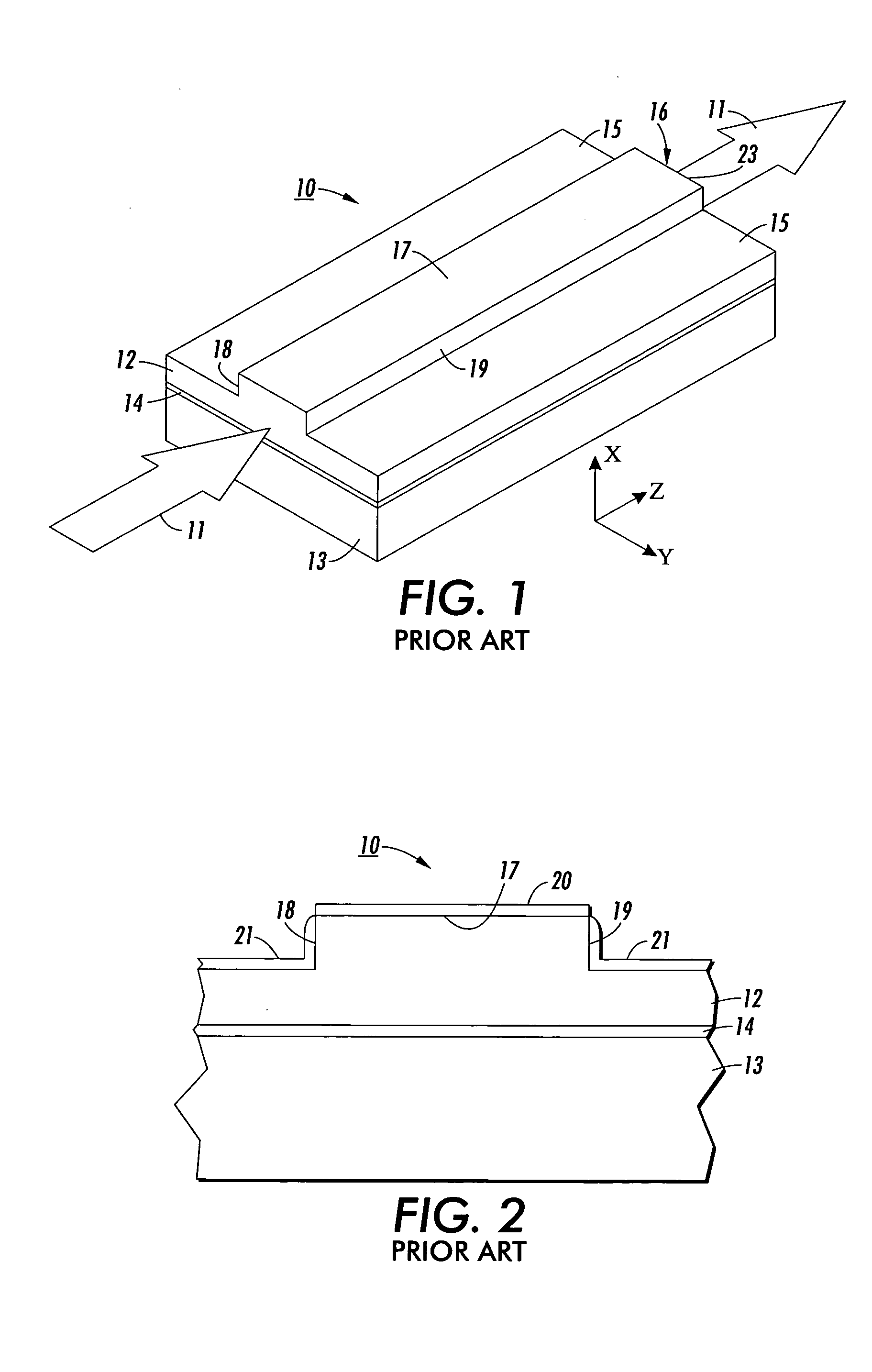
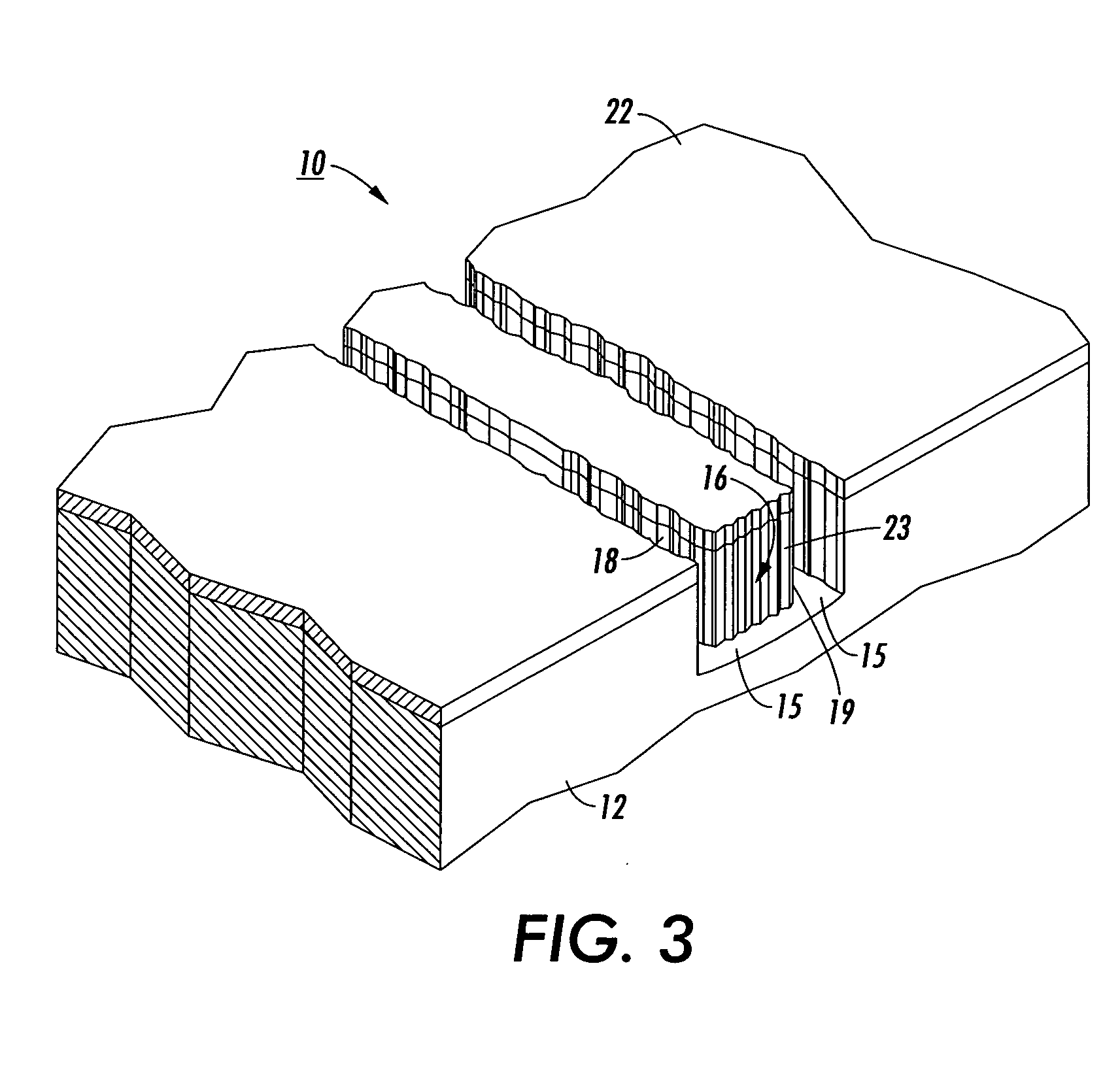
[0018] In FIG. 1, an isometric view of a typical prior art silicon rib waveguide 10 is shown having a coordinate system with axes denoted by x, y, and z. The longitudinal z-axis indicates the direction of light propagation, indicated by the large arrows 11, and the transverse y-direction and x-direction will be referred to as horizontal and vertical direction, respectively. The polarization mode of the propagated light is defined by the magnitude of its transverse electric (E) and transverse magnetic (M) components. If the polarization mode has dominate Ey and Mx components and minor Ex and My fields, the light is called transverse electric (TE) polarized. If the polarization mode has dominate Ex and My fields and minor Ey and Mx components, the light is called transverse magnetic (TM) mode.

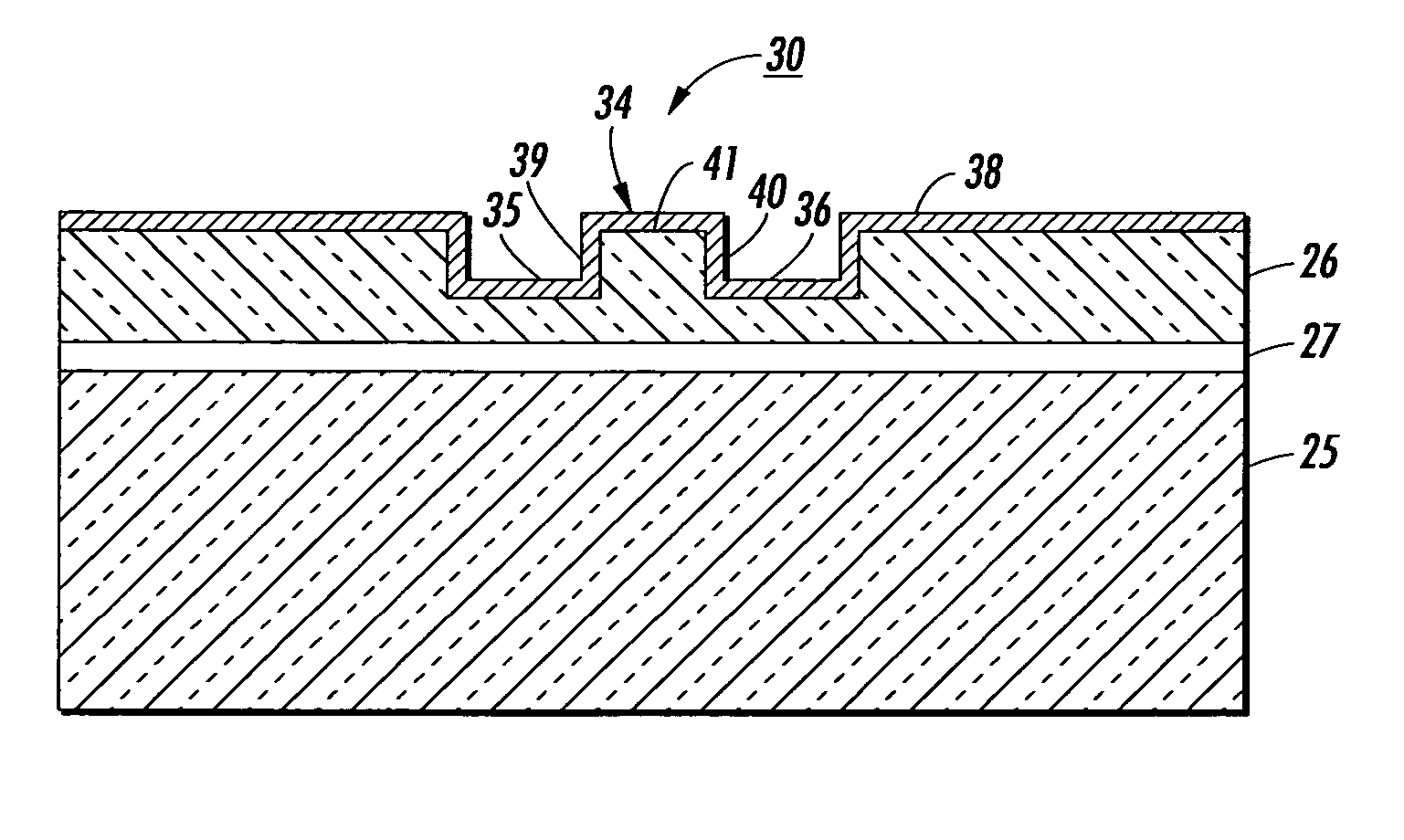
[0019] The waveguide 10 generally consists of an upper silicon substrate 12, usually a single crystal silicon, bonded to a lower usually thicker silicon substrate 13 with a layer of insulative m...


PUM


Abstract

A silicon rib waveguide that has a silicon nitride cladding layer of predetermined thickness to reduce optical loss of light propagating therethrough. An exemplary embodiment of the waveguide is fabricated by using a silicon-on-insulator structure having a single crystal silicon layer bonded to a silicon wafer with a layer of insulative material. An etch resistant masking layer is deposited on the outer surface of the single crystal silicon layer and patterned to produce vias therein. A RIE etching process is used through the vias in the masking layer to form at least one rib bounded by a pair of parallel trenches. The masking layer is removed and a silicon nitride cladding layer is deposited on the rib side and end walls and on the trenches.

Description

BACKGROUND OF THE INVENTION [0001] An exemplary embodiment of this application relates to an improved silicon waveguide for a micro-optical system. More particularly, the exemplary embodiment relates to a silicon rib waveguide having a cladding layer that reduces optical loss due to scattering from waveguide side wall roughness. [0002] In integrated silicon photonic light circuits or micro-optical systems, a silicon waveguide structure is incorporated therein that typically comprises a rib formed in the upper single crystal silicon- layer of a silicon-on-insulator chip or wafer. Light signals may be introduced into and out of the rib waveguide by coupling optical fibers thereto. The rib has a top surface and opposing parallel side walls, and a parallel trench adjacent each of the rib side walls. The rib serves to confine an optical light signal transmitted thereto, and the light signal is contained in the rib and under the trenches as it is transmitted therethrough. [0003] One well ...

Claims


Application Information

Patent Timeline
Patent Type & Authority Applications(United States)
IPC IPC(8): G02B6/13G02B6/12G02B6/136
CPCG02B2006/12097G02B6/136
Inventor KUBBY, JOEL A.WANG, YAO RONG
Owner XEROX CORP
Why Eureka
Try Eureka