

SPM cantilever and fabricating method thereof
- Summary
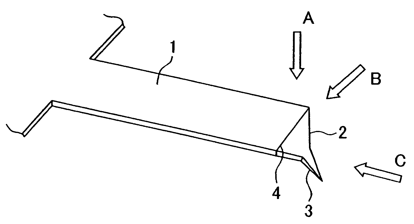
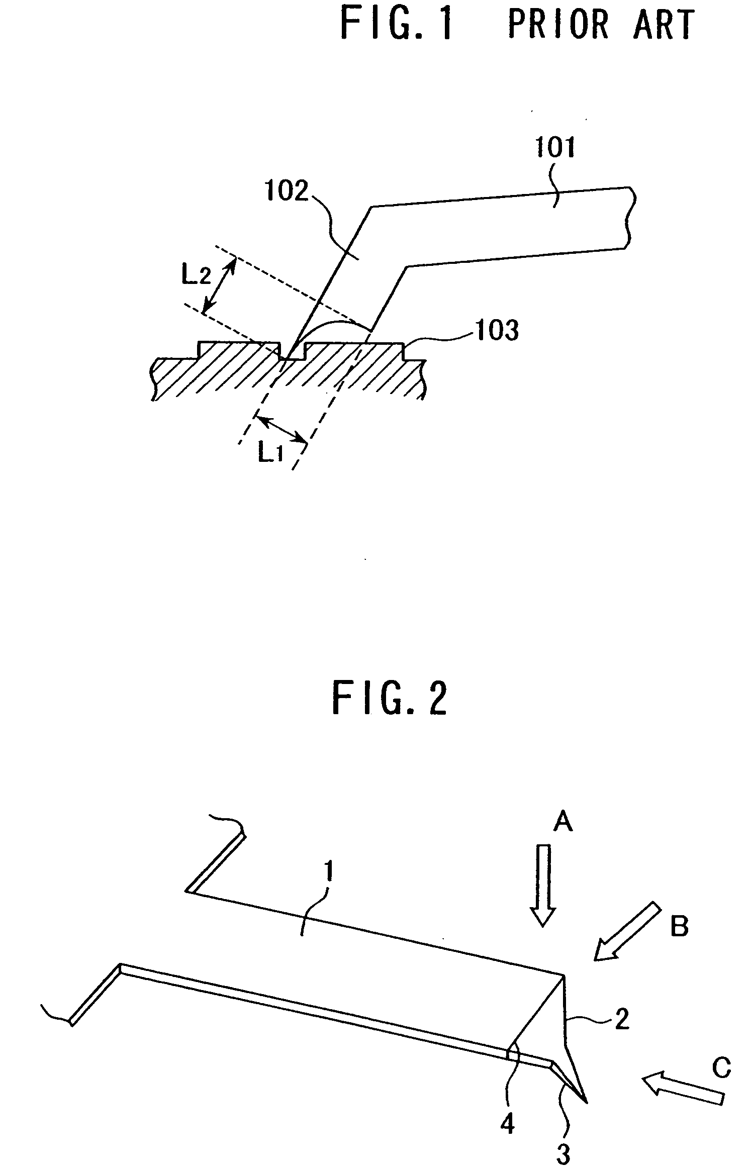
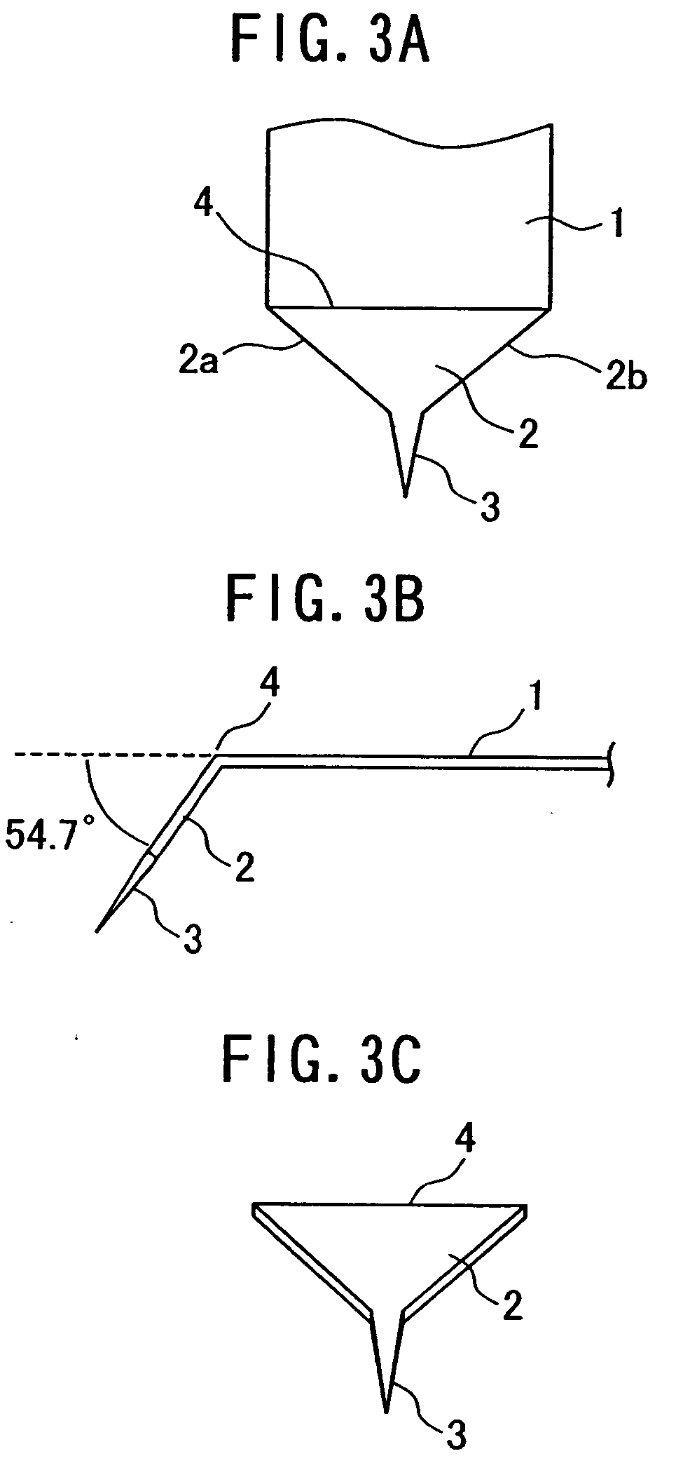
- Abstract
- Description
- Claims
- Application Information
AI Technical Summary
Benefits of technology
Problems solved by technology
Method used
Image

Examples
first embodiment
[0041] The fabricating method of SPM cantilever having the above described construction will now be described by way of the fabricating steps shown in FIGS. 4A to 4I. First, a silicon wafer of lattice plane (100) having Orientation Flat in direction is prepared and used as a substrate 11. As shown in FIG. 4A, then, a mask 12 for the cantilever support portion is formed on the back side of the silicon substrate 11. Here a silicon oxide film for example is suitably used as the mask 12. A mask 13 for forming the probe portion is formed by a silicon nitride film at a predetermined location. At the same time, a silicon nitride film 14 for protecting the cantilever support portion mask 12 is formed on the back side of the silicon substrate 11.
[0042] The silicon front side having the probe portion forming mask 13 thereon is then subjected to anisotropic wet etching by means of an alkali aqueous solution such as KOH (potassium hydroxide) or TMAH (tetramethyl ammonium hydroxide) to form a s...
second embodiment
[0069] The fabricating steps of cantilever will now be described by way of FIGS. 8A to 8K. First, a silicon wafer of lattice plane (100) having Orientation Flat in direction is prepared and used as a substrate 41. Next, as shown in FIG. 8A, a mask 42 for forming the support portion is formed by a silicon oxide film at a predetermined location on the back side of the silicon substrate 41.
[0070] Next, a mask 43 for forming a convex portion is formed on the silicon substrate 41 and, as shown in FIG. 8B, a vertical etching of the silicon substrate front side is effected to a depth of the order of the probe length by Deep-RIE (Reactive Ion Etching) to form a convex portion 44 for forming the probe portion. Here a silicon nitride film is suitably used as the convex portion forming mask 43. Further, at the time of forming the mask 43 of silicon nitride film, a protecting film 45 of silicon nitride film is also formed on the back side of the silicon substrate 41.
[0071] Next, after effect...
PUM
 Abstract
Description
Claims
Application Information