

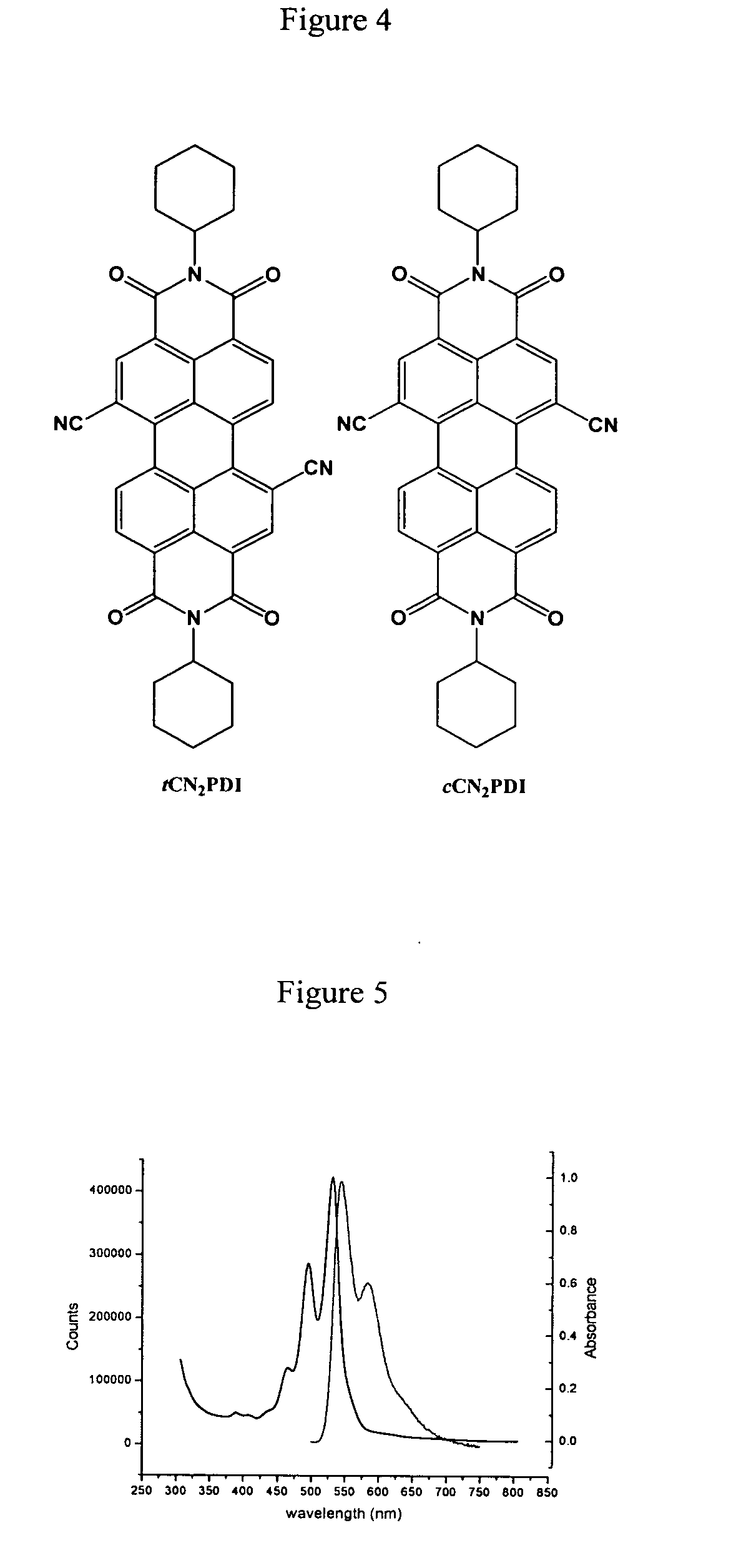
Perylene n-type semiconductors and related devices
a technology of perylene and semiconductors, applied in the field of perylene n-type semiconductors and, can solve the problems of general instability and less than satisfactory solubility characteristics for efficient device fabrication, and achieve the effects of improving solubility and radical anion stability, strong - interaction, and increasing solubility of compound
- Summary
- Abstract
- Description
- Claims
- Application Information
AI Technical Summary
Benefits of technology
Problems solved by technology
Method used
Image

Examples
example 1
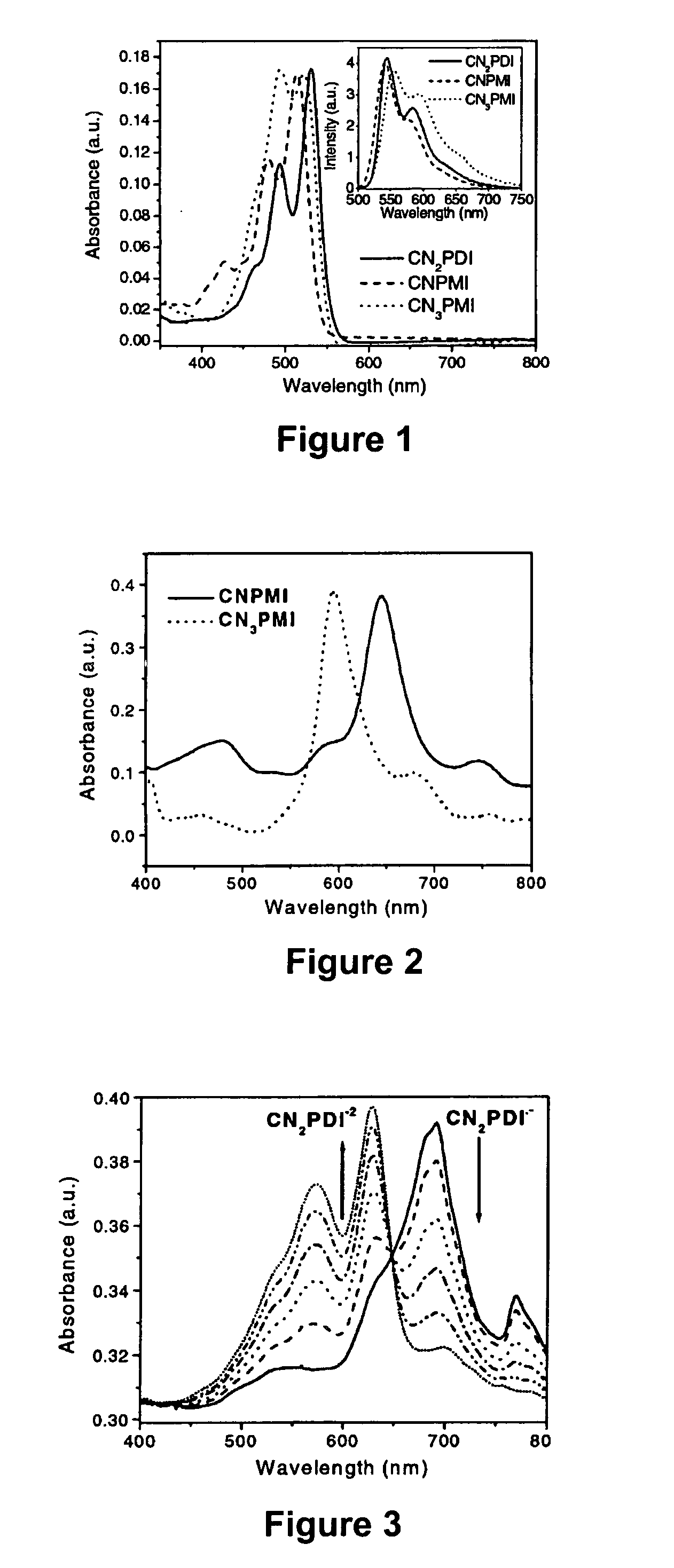
[0063] N,N-bis(cyclohexyl)-1,7-dicyano-perylene-3,4:9,10-bis(dicarboximide) (CN2PDI). N,N-bis(cyclohexyl)-1,7-dibromo-perylene-3,4 :9,10-bis(dicarboximide) (0.048 g, 0.07 mmol), zinc cyanide (0.065 g, 0.55 mmol), 1,1′-bis(diphenylphosphino)-ferrocene (0.005 g, 0.01 mmol) and tris(dibenzylideneacetone)-dipalladium(0) (0.010 g, 0.01 mmol) were combined in 4 ml p-dioxane and refluxed for 19 hours under a nitrogen atmosphere. The crude product was diluted with chloroform, filtered through Celite, and the solvent removed on a rotary evaporator. The crude product was chromatographed on a silica column using 98% DCM / 2% acetone as the eluent to yield 0.041 g product CN2PDI (theory 0.041 g, quantit). 1H NMR (CDCl3): 9.692 (d, J=8.1 Hz, 2H), 8.934 (s, 2H), 8.888 (d, J=8.1 Hz, 2H), 5.025 (m, 2H), 2.533 (m, 4H), 1.931 (m, 4H), 1.755 (m, 6H), 1.504 (m, 4H), 1.329 (m, 2H). M.S.(EI) : Calcd. for C38H28N4O4: 604.2105, Found: 604.2108.
example 2
[0064] N-(2,5-di-tert-butylphenyl)-9-cyano-1,6-bis(3,5-di-tert-butylphenoxy)-perylene-3,4-dicarboximide (CNPMI). N-(2,5-di-tert-butylphenyl)-9-bromo-1,6-bis(3,5-di-tert-butylphenoxy)-perylene-3,4-dicarboximide (0.100 g, 0.10 mmol), zinc cyanide (0.047 g, 0.40 mmol), 1,1′bis(diphenylphosphino)-ferrocene (0.009 g, 0.02 mmol) and tris(dibenzylideneacetone)-dipalladium(0) (0.003 g, 0.003 mmol) were combined in 10 ml p-dioxane in a 25 ml round-bottom flask and heated to reflux for 36 hours under a N2 atmosphere. Upon cooling to room temperature, the crude reaction mixture was diluted with chloroform, washed twice with water, and the solvent removed on a rotary evaporator. The crude product was flash chromatographed on a silica column using a 65% hexanes / 35% chloroform mixture as the eluent to afford 0.094 g product (CNPMI) (theory 0.094 g, quantitative). 1H NMR (CDCl3): 9.525 (d, J=8.7 Hz, 1H), 9.422 (d, J=8.2 Hz, 1H), 8.342 (d, J=7.4 Hz, 1H), 8.281 (s, 2H), 8.021 (d, J=8.2 Hz, 1H), 7.84...
example 3
[0065] N-(2,5-di-tert-butylphenyl)-1,6,9-tricyano-perylene-3,4-dicarboximide (CN3PMI). N-(2,5-di-tert-butylphenyl)-1,6,9-tribromo-perylene-3,4-dicarboximide (0.082 g, 0.11 mmol), zinc cyanide (0.156 g, 1.33 mmol), 1,1′bis(diphenylphosphino)-ferrocene (0.009 g, 0.02 mmol) and tris(dibenzylideneacetone)-dipalladium(0) (0.004 g, 0.004 mmol) were added to 5 ml p-dioxane and heated to reflux for 16 hours under a N2 atmosphere. The reaction mixture was diluted with methylene chloride, filtered through Celite, and the solvent removed on a rotary evaporator. The crude product was flash chromatographed on a silica column using methylene chloride as the eluent to give 0.062 g product CN3PMI (theory 0.064g, 97%). 1H NMR (CDCl3): 9.603 (d, J=8.8 Hz, 1H), 9.532 (d, J=7.3 Hz, 1H), 9.048 (s, 2H), 8.638 (d, J=7.3 Hz, 1H), 8.248 (d, J=7.3 Hz, 1H), 8.096 (t, J=7.3 Hz, 1H), 7.608 (d, J=8.8 Hz, 1H), 7.495 (d, J=8.8 Hz, 1H), 6.967 (s, 1H), 1.328 (s, 9H), 1.283 (s, 9H). M.S.(EI): Calcd. for C39H28N4O2: 5...
PUM
| Property | Measurement | Unit |
|---|---|---|
| thick | aaaaa | aaaaa |
| tilt angle | aaaaa | aaaaa |
| temperature | aaaaa | aaaaa |
Abstract
Description
Claims
Application Information