
Organic electroluminescence device and organic electroluminescence display

Inactive Publication Date: 2005-08-18
FUJIFILM HLDG CORP +1
View PDF6 Cites 27 Cited by
  • Summary
  • Abstract
  • Description
  • Claims
  • Application Information

AI Technical Summary

Benefits of technology

[0014] A more specific object of the present invention is to provide an organic electroluminescence device that has excellent luminous efficiency and that is able attain a long life-span.
[0019] With the present invention, the amount of electron current injected into the luminescent layer can be increased by providing the carrier transport multilayered body having alternate layers of the first carrier transport layer and the second carrier transport layer having different electron affinities between the luminescent layer and the cathode. As a result, the organic electroluminescence device of the present invention attains a high luminous efficiency and a long life-span by balancing the amount of electron current and the amount of hole current.
[0020] The first carrier transport layer and the second carrier transport layer have different electron affinities. Owing to the different electron affinities of the first carrier transport layer and the second carrier transport layer, multiple quantum wells can be formed and the amount of electron current can be increased. It is to be noted that electron affinity is expressed as an energy difference between an energy of a lower end of a conductive member of a material included in, for example, the carrier transport layer and a vacuum level, and is indicated as a positive value.
[0022] With the present invention, an organic electroluminescence display having high luminous efficiency and a long life-span can be obtained.

Problems solved by technology

In employing the organic EL display for practical use, however, a task of obtaining a longer life-span for the organic EL display is yet to be achieved.
Nevertheless, when a low work function simple metal, alloys or LiF, for example, is used in the cathode 18, the amount of electron current reaching the luminescent layer 15 becomes less than the amount of hole current, thereby causing unevenness in the amount of current between the electrons and the holes.
This causes the current of the holes not contributing to illumination to become wasted and prevents a sufficient luminous efficiency from being obtained.
However, an excess application of voltage is liable to cause a chemical reaction at interfaces between the anode 12 and the hole injection layer 13 and between the cathode 18 and the electron transport layer 16.
This leads to property change and function deterioration in the hole injection layer 13 and the electron transport layer 16, and furthermore, device failure.
Therefore, there is a problem in obtaining a sufficient life-span for the device.
However, this document does not disclose a specific configuration of the structure of the multilayer electron transport area.

Method used


Image

  • Organic electroluminescence device and organic electroluminescence display
  • Organic electroluminescence device and organic electroluminescence display
  • Organic electroluminescence device and organic electroluminescence display

Examples


first embodiment

(First Embodiment)

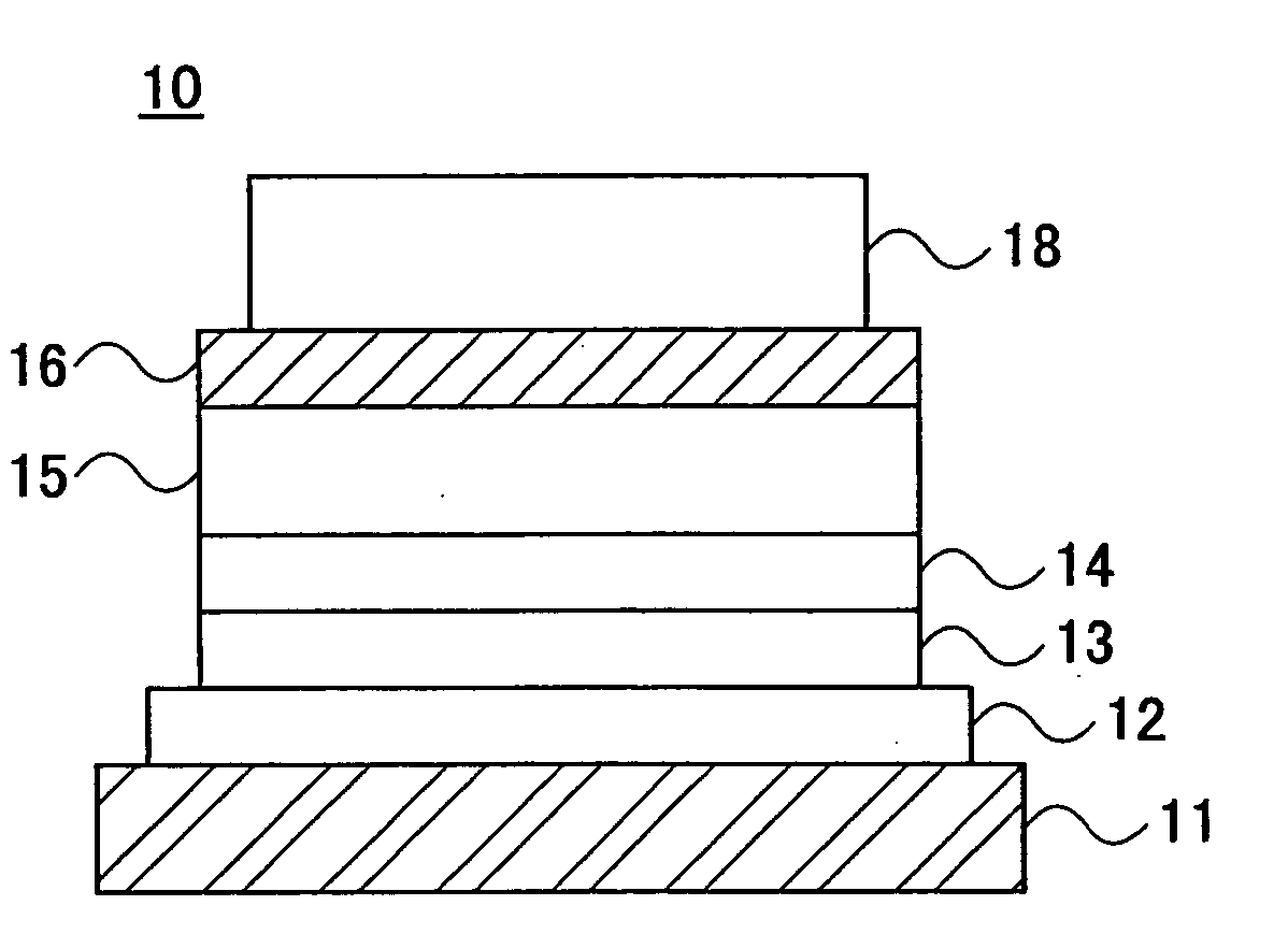
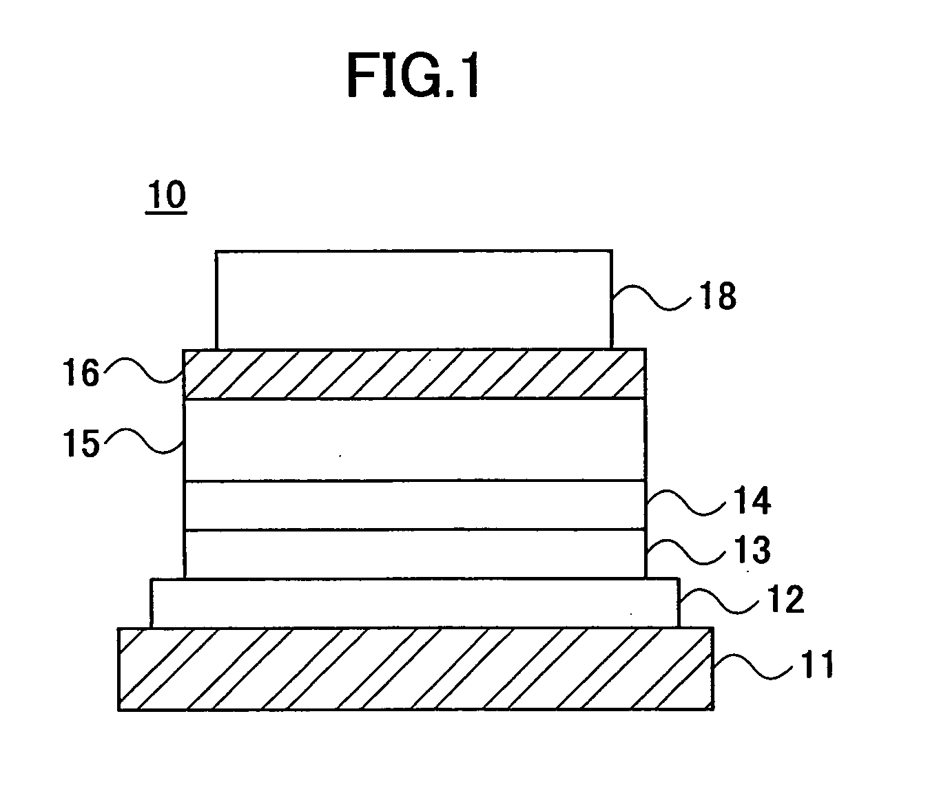
[0043] Embodiments of the present invention of an organic EL device are described with reference to the accompanying drawings.

[0044] FIG.4 is a cross-sectional view showing an organic EL device according to an embodiment of the present invention. FIG.5 is an example of an energy diagram of an organic EL device according to the embodiment shown in FIG.4. In FIG.5, “Ea” indicates electron affinity, “Eg” indicates energy gap, and “Ip” indicates ionization potential. With reference to FIGS. 4 and 5, according to this embodiment, an organic EL device 30 has a transparent substrate 31, an anode 32, a hole injection layer 33, a hole transport layer 34, a luminescent layer 35, an electron transport multilayered body 36, a cathode-side electron transport layer 37, and a cathode 38 which are formed in that order on the substrate 31.

[0045] For example, a transparent insulating substrate such as glass or quartz, a semiconductor substrate such as Si, a film such as PET or PEN...

example 1

[0069] An anode with a thickness of 150 nm is formed on a glass substrate by a sputtering method with use of ITO, and is subject to UV ozone processing in which the anode surface is irradiated with UV rays under an oxygen atmosphere for 20 minutes. Then, 2-TNATA (thickness 40 nm) serving as the hole injection layer, α-NPD (thickness 10 nm) serving as the hole transport layer, and TYG 201 (thickness 20 nm) serving as the luminescent layer, are formed in order.

[0070] Next, starting from TYE 704, the formation of a combination of TYE 704 (thickness 15 nm) and TYG 201 (thickness 15 nm), serving as the electron transport multilayered body, is repeated twice. Furthermore, a single layer of TYE 704 (thickness 20 nm) is formed on the electron transport multilayered body, and the cathode formed of LiF / Al is last formed.

[0071] In the organic EL device in this example, a green luminescence is observed in a case where voltage is no less than 3 V. When voltage of 10 V is applied, luminance of ...

second example

[0072] The organic EL element of this example is the same as that of the first example except for repeating the formation of a combination of TYE 704 (thickness 10 nm) and TYG 201 (thickness 10 nm) for three times.

[0073] In the organic EL device in this example, a green luminescence is observed in a case where voltage is no less than 3 V. When voltage of 10 V is applied, luminance of 1075 cd / m2 and a luminous efficiency of 9.70 cd / A are obtained.


PUM


Abstract

An organic EL device includes a transparent substrate (31), an anode (32), a hole injection layer (33), a hole transport layer (34), an luminescent layer (35), an electron transport multilayered body (36), a cathode-side electron transport layer (37), and a cathode (38) formed on the substrate (31) in that order. The electron transport multilayered body (36) includes alternate layered two kinds of electron transport layers (36A, 36B) having electron affinities that are different from each other. Increasing the amount of electron current injected from the cathode (38) for balancing with the amount of hole current, and enhancing luminous efficiency.

Description

CROSS-REFERENCE TO RELATED APPLICATIONS [0001] This application is a U.S. continuation application filed under 35 USC 111(a) claiming benefit under 35 USC 120 and 365(c) of PCT application JP 2003 / 003027, filed Mar. 13,2003. The foregoing application is hereby incorporated herein by reference.BACKGROUND OF THE INVENTION [0002] 1. Field of the Invention [0003] The present invention generally relates to an electroluminescence device and a flat panel display using an electroluminescence device, and more particularly to an organic electroluminescence device and an organic electroluminescence display. [0004] 2. Description of the Related Art [0005] In recent years, demands of the market are shifting from a conventional large size and heavy-weight CRT (Braun tube) display to a thin-size and light-weight flat display. As for the flat displays, there are liquid crystal displays and plasma displays which are employed, for example, as home television receivers and monitors of personal compute...

Claims


Application Information

Patent Timeline
IPC IPC(8): H01L51/00H01L51/50H05B33/00H05B33/14H05B33/22
CPCH01L51/0059H01L51/006H01L51/5048H01L51/0078H01L51/0081H01L51/0077H10K85/633H10K85/311H10K85/631H10K85/30H10K85/324H10K50/14
Inventor NAKAYAMA, MASAYAITAI, YUICHIROKINOSHITA, MASARUKODAMA, JUN
Owner FUJIFILM HLDG CORP
Features
  • Generate Ideas
  • Intellectual Property
  • Life Sciences
  • Materials
  • Tech Scout
  • Unparalleled Data Quality
  • Higher Quality Content
  • 60% Fewer Hallucinations
Learn More