Semiconductor circuit device

a technology of semiconductor circuit devices and circuits, applied in the direction of logic circuit coupling/interface arrangement, power consumption reduction, pulse technique, etc., can solve the problems of reducing the working speed of the circuit, reducing the operating current, and reducing the size of the transistor to control the source node of the transistor driving the signal line, so as to reduce the size of the transistor to control the source node of the transistor. the effect of reducing the size of the transistor

Active Publication Date: 2005-08-25
LONGITUDE LICENSING LTD
View PDF6 Cites 10 Cited by
  • Summary
  • Abstract
  • Description
  • Claims
  • Application Information

AI Technical Summary

Benefits of technology

[0040] A first advantage of the present invention is to drive a signal line of a signal line driving circuit in a semiconductor circuit device with low-voltage-swing at high speed. The reason is that the signal line driving circuit includes a low-threshold transistor. Thus, OFF-state current is sufficiently low and ON-state current is sufficiently high.
[0041] A second advantage of the present invention is to lower standby current in the signal line driving circuit. The reason is that the potential diffe

Problems solved by technology

Due to higher-density integration, larger-scale integration and higher speed of recent semiconductor circuit devices, an increase of operating current and resultant generation have caused serious problem to occur in each semiconductor circuit device.
An important challenge is to reduce the operating current.
Unfortunately, when a supply voltage is merely lowered, the working speed of a circuit is lowered.
Disadvantageously, however, the low voltage VCC leads to a reduction in working speed of the circuit block.
Unfortunately, when the threshold voltage of each tra

Method used


Image

  • Semiconductor circuit device
  • Semiconductor circuit device
  • Semiconductor circuit device

Examples


first embodiment

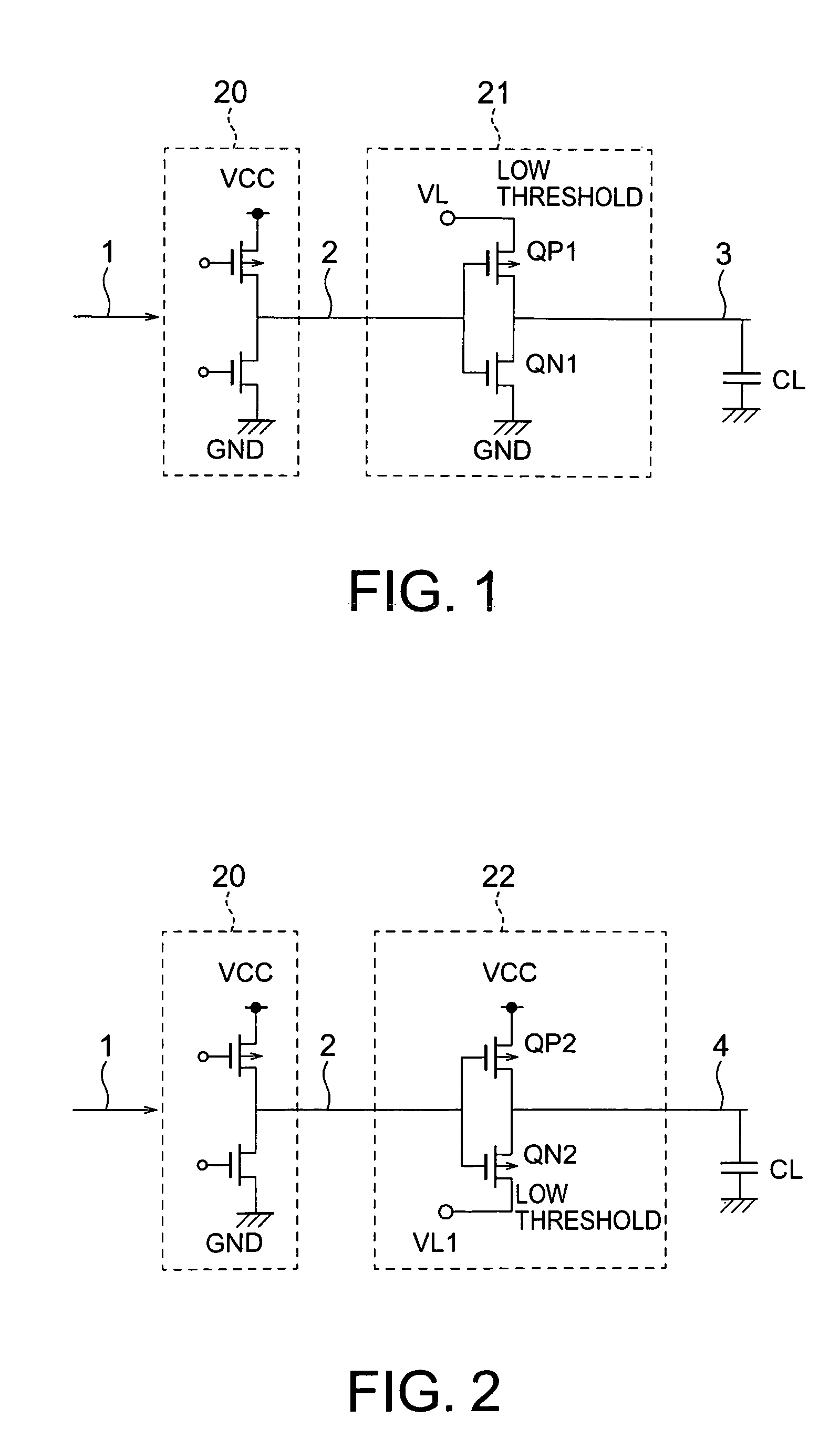
[0059]FIG. 1 shows a circuit block according to a first embodiment of the present invention. The circuit block includes a CMOS circuit including a logic circuit 20 and a signal line driving circuit 21. The logic circuit 20 is arranged between a power supply VCC and ground GND. The logic circuit 20 is a CMOS logic circuit including normal-threshold transistors. The logic circuit 20 performs a logic operation on a signal supplied from an input signal line 1 and generates an output signal in a high level VCC or a low level GND to a node 2.

[0060] The signal line driving circuit 21 is a CMOS inverter including an NMOS transistor QN1 and a PMOS transistor QP1. The source of the NMOS transistor QN1 is connected to the ground as a negative power supply, the gate is connected to the node 2, and the drain is connected to an output signal line 3. The source of the PMOS transistor QP1 is connected to an internal power supply VL as a positive power supply, the gate is connected to the node 2, a...

second embodiment

[0073]FIG. 2 is a diagram of a circuit block according to a second embodiment of the present invention. FIG. 6 is a timing chart of the operation according to the second embodiment. A signal line driving circuit 22 according to the second embodiment is an inverter including an NMOS transistor QN2 and a PMOS transistor QP2. The source of the NMOS transistor QN2 is connected to an internal power supply VL1, the gate is connected to a node 2, and the drain is connected to an output signal line 4. The source of the PMOS transistor QP2 is connected to a power supply VCC, the gate is connected to the node 2, and the drain is connected to the output signal line 4. The signal line driving circuit 22 buffers a signal supplied from the node 2 and generates the signal to the output signal line 4. The NMOS transistor QN2 defines a low output level. The PMOS transistor QP2 defines a high output level. A logic circuit 20 is the same as that in FIG. 1. The potential of the internal power supply VL...

third embodiment

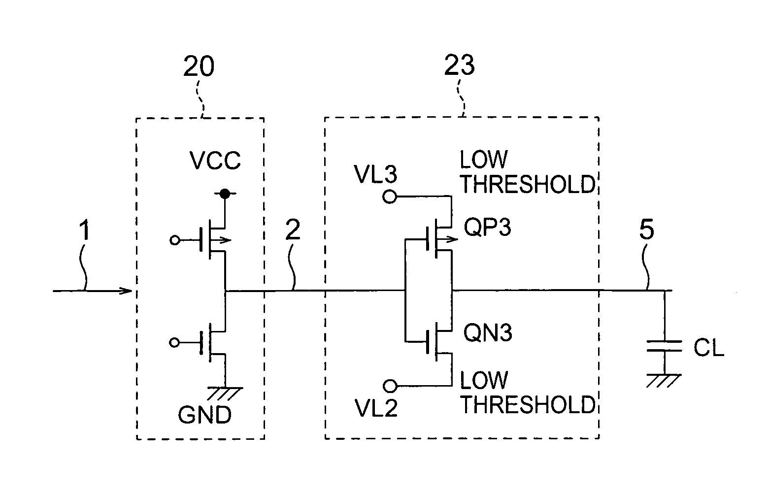
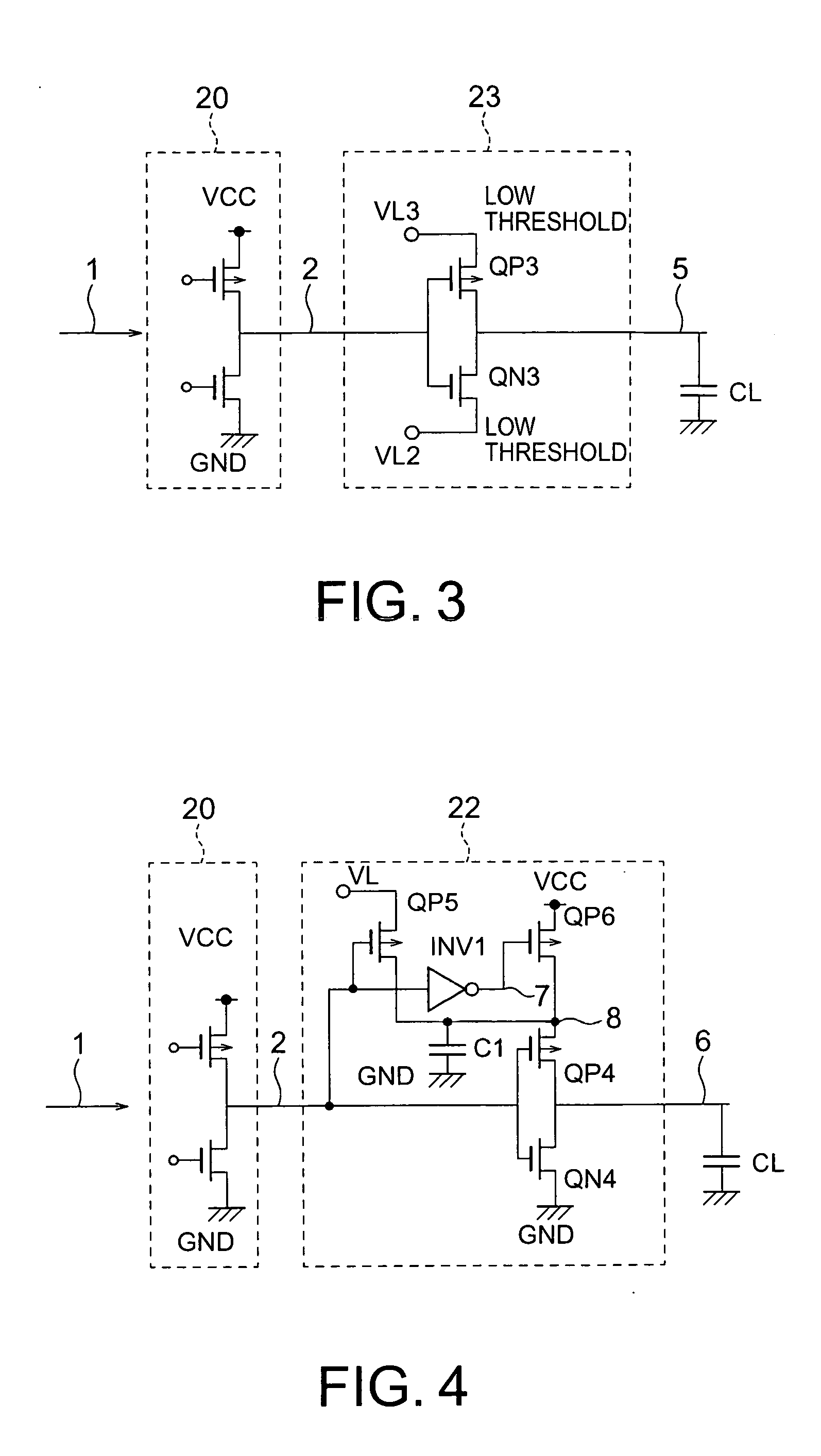
[0078]FIG. 3 is a diagram of a circuit block according to a third embodiment of the present invention. FIG. 7 is a timing chart of the operation according to the third embodiment. The circuit block according to the third embodiment includes a logic circuit 20 and a signal line driving circuit 23. The signal line driving circuit 23 is an inverter including an NMOS transistor QN3 and a PMOS transistor QP3. The source of the NMOS transistor QN3 is connected to an internal power supply VL2, the gate is connected to a node 2, and the drain is connected to an output signal line 5. The source of the PMOS transistor QP3 is connected to an internal power supply VL3, the gate is connected to the node 2, and the drain is connected to the output signal line 5. The signal line driving circuit 23 buffers a signal supplied from the node 2 and generates the signal to the output signal line 5. The NMOS transistor QN3 defines a low output level and the PMOS transistor QP3 defines a high output level....


PUM


Abstract

The present invention relates to a semiconductor circuit device including a logic circuit and a signal line driving circuit. The logic circuit is operated at high supply voltage and outputs a signal with a high voltage amplitude. The signal line driving circuit receives a lower supply voltage and has a low-threshold transistor. With the above configuration, a signal can be transmitted at a high speed with a low voltage amplitude and low power consumption. Thus, the semiconductor circuit device including the signal line driving circuit can reduce operating current and can be operated with a low amplitude and low standby current at a high speed.

Description

[0001] This application claims priority to prior Japanese patent application JP 2004-43300, the disclosure of which is incorporated herein by reference. BACKGROUND OF THE INVENTION [0002] 1. Field of the Invention [0003] The present invention relates to semiconductor circuit devices with signal line driving circuits and, more particularly, to a semiconductor circuit device including signal line driving circuits for transferring a signal between circuit blocks with low power, low-voltage-swing, and low current consumption at high speed. [0004] 2. Description of the Related Art [0005] Due to higher-density integration, larger-scale integration and higher speed of recent semiconductor circuit devices, an increase of operating current and resultant generation have caused serious problem to occur in each semiconductor circuit device. An important challenge is to reduce the operating current. One approach to the challenge is to lower an external supply voltage or an internal reduced suppl...

Claims


Application Information

Patent Timeline
IPC IPC(8): H01L27/04H01L21/822H03K19/00H03K19/017H03K19/0175H03K19/0185H03K19/094
CPCH03K19/0013H03K19/018521H03K19/01707H03K19/0027
Inventor TSUKADA, SHUICHI
Owner LONGITUDE LICENSING LTD
Why Eureka
Try Eureka