Semiconductor device

a semiconductor memory and semiconductor technology, applied in semiconductor devices, digital storage, instruments, etc., can solve the problems of large area, large area, and fear of mos transistor destruction, and achieve the effect of small area, large area, and high curren

a semiconductor memory and semiconductor technology, applied in semiconductor devices, digital storage, instruments, etc., can solve the problems of large area, large area, and fear of mos transistor destruction, and achieve the effect of small area, large area, and high curren

US20050185445A1Inactive Publication Date: 2005-08-25RENESAS ELECTRONICS CORP

Image

  • Semiconductor device
  • Semiconductor device
  • Semiconductor device

Examples


Embodiment Construction

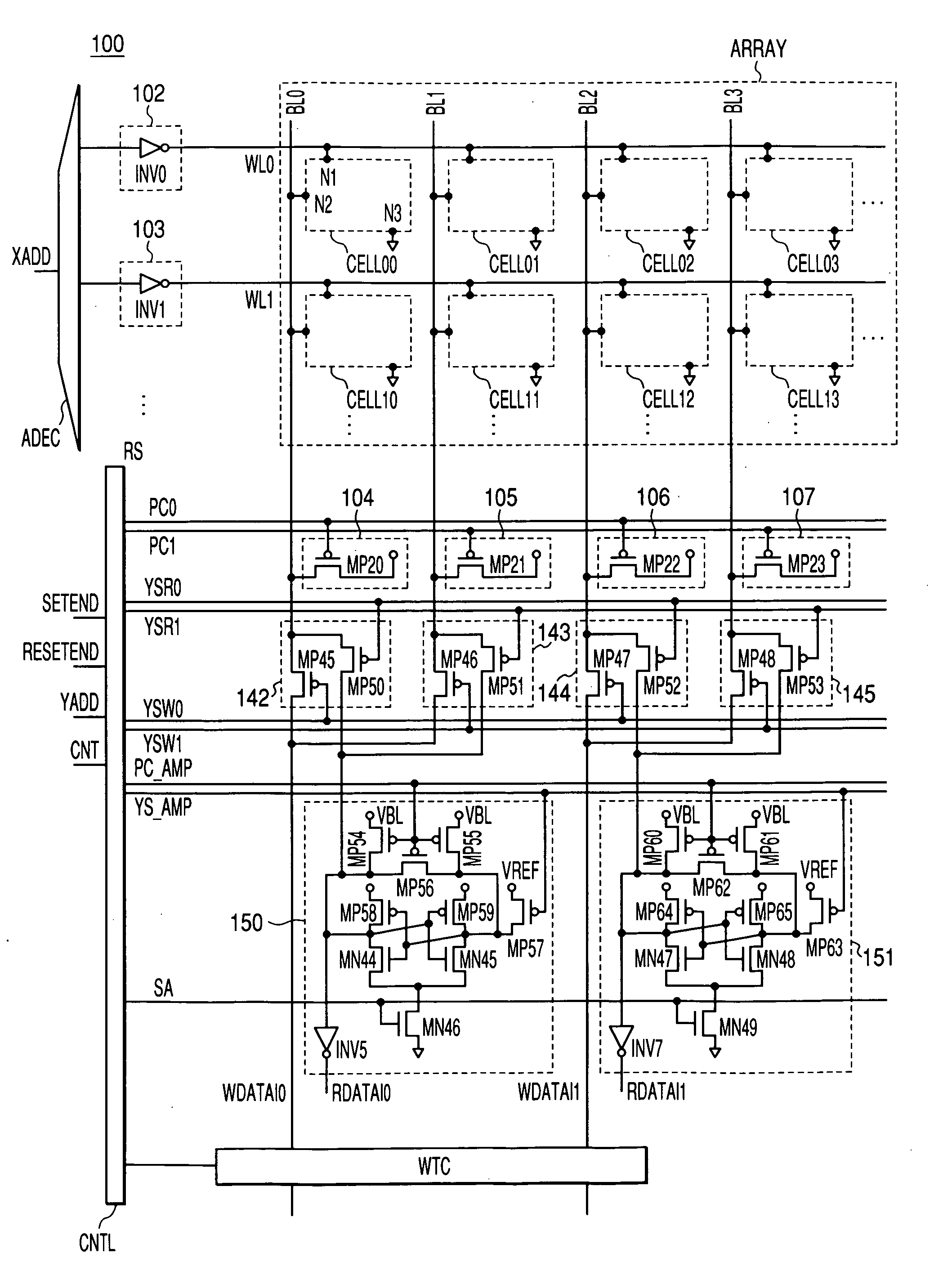
[0055] Preferred embodiments of a semiconductor memory device according to the present invention will hereinafter be described with reference to the drawings. In each of the embodiments, though there is particular no limit to the configuration, those circuitry elements of each functional block are formed on a single semiconductor substrate (with a material such as single crystal silicon, etc.), using an integrated circuit technology of well-know CMOS (complementary MOS) transistors or the like. In the drawings of the MOS transistors, the connection to the substrate potential is not particularly shown. As long as the MOS transistors are properly operable, their connection system is not particularly restricted. Unless otherwise indicated, “L” denotes a low level of a signal, while “H” denotes a high level of a signal.

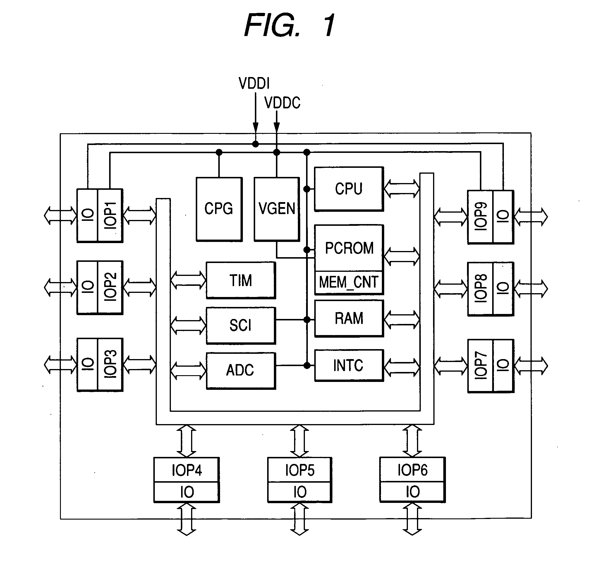
[0056]FIG. 1 is a diagram showing an example of a single-chip microcomputer according to the present invention. Although though is no particular limit to the configurati...


PUM


Abstract

A semiconductor device comprises a plurality of memory cells, a central processing unit, a timer circuit which times a RESET time, and a timer circuit which times a SET time. A threshold voltage of an NMOS transistor of each memory cell is lower than that of the peripheral circuit, thereby easily executing a RESET operation. The direction of a flowing current is changed across the RESET operation and the SET operation, and the bit lines are activated at high speed, thus preventing system malfunctions. Further, the semiconductor device can overcome such problems as a wrong write operation and data destruction, resulting from the variation in the CMOS transistors when operating phase change elements with minimum size CMOS transistors at a core voltage (e.g. 1.2 V). According to the present invention, stable operations can be realized at a low voltage, using minimum-size cell transistors.

Description

CLAIM OF PRIORITY [0001] The present application claims priority from Japanese application JP 2004-043948 filed on Feb. 20, 2004, and Japanese application JP 2005-001979 filed on Jan. 7, 2005, the content of which are hereby incorporated by reference into this application. FIELD OF THE INVENTION [0002] The present invention relates to a semiconductor device and a semiconductor memory device, and more particularly to a system LSI (a microcomputer) having a hybrid mounting approach with a non-erasable memory and / or a nonvolatile memory. BACKGROUND OF THE INVENTION [0003] To achieve a high-integrated nonvolatile memory operable at high speed, a phase change memory has continuously been developed. Such a phase change memory is described in Non-patent documents 1, 2, and 3 and Patent document 1. For example, the phase change memory of Non-patent document 1 stores information, by taking advantage of a characteristic that the resistance of a phase change material (a chalcogenide material) ...

Claims


Application Information

Patent Timeline
25 Aug 2005
Publication
US20050185445A1
IPC
G06F13/00; G11C11/00; G11C13/00; G11C16/02; G11C16/10; G11C16/26; G11C16/34; G11C19/08; H01L27/10; H01L27/105
CPC
G11C13/0004; G11C13/0033; G11C13/004; G11C2213/82; G11C13/0069; G11C16/3454; G11C2013/0092; G11C13/0064
Inventors
OSADA, KENICHI; TAKEMURA, RIICHIRO