Substrate for mounting IC chip, multilayered printed circuit board, and device for optical communication

a multi-layered printed circuit board and substrate technology, applied in the direction of instruments, cladded optical fibres, optical elements, etc., can solve the problems of large distance of electric wirings and large size of overall devices, and achieve excellent connection reliability and low connection loss

Inactive Publication Date: 2005-08-25
IBIDEN CO LTD
View PDF15 Cites 131 Cited by
  • Summary
  • Abstract
  • Description
  • Claims
  • Application Information

AI Technical Summary

Benefits of technology

[0020] Among them, preferably the light receiving element and the light emitting element are {circle over (1)} or {circle over (2)} for the following reasons. The light receiving element and the light emitting element (light receiving part and light emitting part) can be accurately positioned to the light introducing paths (optical waveguides or the like) of an external substrate such as a motherboard using the self-alignment effect of solders. Therefore, it is possible to ensure excellent positioning accuracy for the light receiving element and the light emitting element. In addition, since it is unnecessary to employ wire-bonding, it is possible to easily mount these elements on the substrate for mounting an IC chip. The light receiving element and the light emitting element mounted on the substrate for mounting an IC chip according to the first group of the present invention are not necessarily limited to one kind of those mentioned in {circle over (1)} to {circle over (4)} but two or more of them in {circle over (1)} to {circle over (4)} may be used in combination.
[0039] In addition, when the optical waveguide having the optical path conversion mirror formed in advance is bonded to the substrate or the interlaminar insulating layer during the formation of the optical waveguide, it is possible for the elastic material layer to moderate stress applied to the optical waveguide and to prevent scratches, cracks and the like from occurring to the optical waveguide.
[0046] The reason is considered to be because: it has been unsuccessful to fully ensure the factor for accomplishing optical communication that is excellent in connection reliability, i.e., low connection loss in the connection among the optical components (connection between the optical fiber and the optical waveguide, connection between the optical waveguide and the light receiving element or light emitting element and the like).

Problems solved by technology

Since the IC mounting package substrate and the optical components are equipped separately with the above-described conventional terminal device, the size of the overall device becomes large.
Therefore, the distance of the electric wirings becomes large, whereby a signal error or the like due to cross-talk noise or the like tends to occur during the transmission of a signal.

Method used


Image

  • Substrate for mounting IC chip, multilayered printed circuit board, and device for optical communication
  • Substrate for mounting IC chip, multilayered printed circuit board, and device for optical communication
  • Substrate for mounting IC chip, multilayered printed circuit board, and device for optical communication

Examples


example 1

[1084] A. Production of Resin Film for Interlaminar Insulating Layer

[1085] 30 parts by weight of bisphenol A-type epoxy resin (epoxy equivalent: 469, Epicoat 1001 made by Yuka Shell Epoxy Co., Ltd.), 40 parts by weight of cresol-novolac type epoxy resin (epoxy equivalent: 215, Epiclon N-673 made by Dainippon Ink and Chemicals, Inc.), and 30 parts by weight of triazine structure containing phenol-novolac resin (phenol hydroxyl group equivalent: 120, Phenolite KA-7052 made by Dainippon Ink and Chemicals, Inc.) were dissolved while being heated in 20 parts by weight of ethyl diglycol acetate and 20 parts by weight of solvent naphtha under stirring condition, followed by the addition of 15 parts by weight of epoxy-terminated polybutadiene rubber (Denalex R-45EPT made by Nagase Kasei Corp.) and 1.5 parts by weight of a pulverized product of 2-phenyl-4,5-bis(hydroxymethyl)imidazole, 2 parts by weight of a finely pulverized silica, and 0.5 parts by weight of a silicon based defoaming agen...

example 2

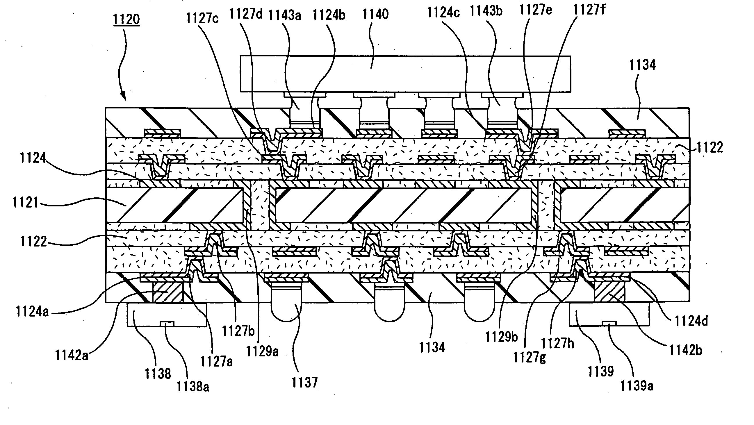
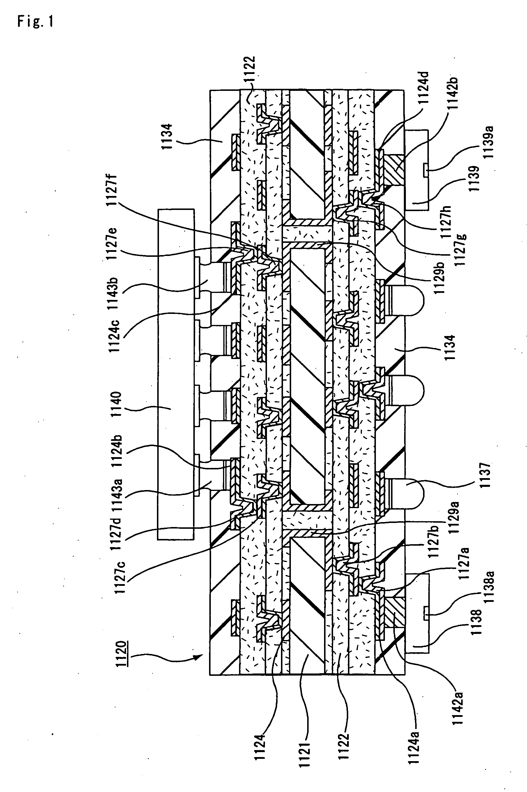
[1123] (1) First, a substrate having interlaminar insulating layers and conductor circuits built up on each surface of the substrate was manufactured in the similar manners as those in the steps (1) to (14) of Example 1.

[1124] (2) Next, solder resist composition layers were formed in the similar manners to those in the steps (15) and (16) of Example 1.

[1125] (3) A 5 mm-thick photomask drawing a pattern of openings for forming solder bump was firmly stuck to the solder resist composition layers on the side which the IC chip was mounted, followed by the exposure to UV rays of 1000 mJ / cm2 dose and development with the DMTG solution to form openings having 200 μm diameter.

[1126] A photomask drawing patterns of the openings for forming solder bump and openings for housing optical elements was firmly stuck to each solder resist composition layer on the side which the optical elements were mounted, followed by exposure and development under the above-mentioned conditions, thereby formin...

example 3

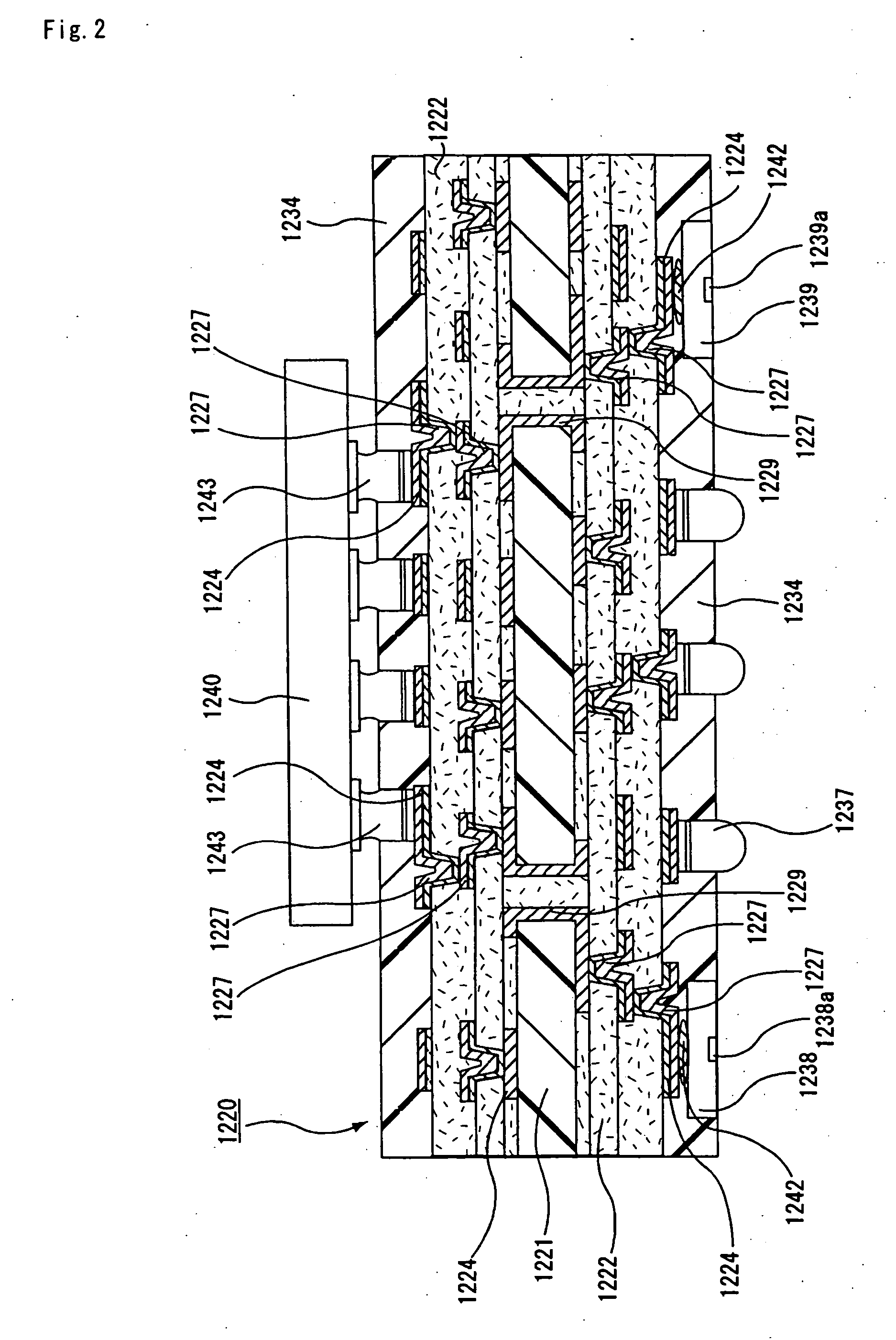
[1131] (1) First, a substrate having interlaminar insulating layers and conductor circuits built up on each surface of the substrate was manufactured in the same manners as those in the steps (1) to (14) of Example 1.

[1132] (2) Next, a light receiving element and a light emitting element were attached to their respective predetermined positions of the conductor circuit on the outermost layer through conductive adhesive. The same light receiving element and light emitting element as those used in Example 1 were used.

[1133] (3) A solder resist composition was prepared in the same manner as that in the step (15) of Example 1.

[1134] Further, after bonding a resist to the light receiving portion of the light receiving element and the light emitting portion of the light emitting element attached to the conductor circuit in the step (2) above, the solder resist composition was applied and drying treatments were conducted at 700 for 20 minutes and at 700 for 30 minutes, respectively, the...


PUM


Abstract

The present invention provides a device for optical communication comprising: a substrate for mounting an IC chip having a light emitting element and a light receiving element mounted at predetermined positions; and a multilayered printed circuit board having an optical waveguide formed at a predetermined position, which is low in connection loss among the mounted optical components and which has excellent connection reliability. The device for optical communication according to the present invention comprises the substrate for mounting an IC chip and the multilayered printed circuit board, wherein the substrate for mounting an IC chip includes conductor circuits, interlaminar insulating layers and via-holes for connecting the conductor circuits, with the interlaminar insulating layers interposed therebetween, to each other, and a light receiving element and a light emitting element are mounted on the substrate for mounting an IC chip.

Description

TECHNICAL FIELD [0001] The present invention relates to a substrate for mounting an IC chip, a multilayered printed circuit board and a device for optical communication. BACKGROUND ART [0002] Recently, attention has been focused on optical fibers mainly in communication fields. Particularly in the IT (Information Technology) field, a communication technique of employing the optical fibers is necessary to provide a high speed Internet network. [0003] The optical fiber has features: (1) low loss, (2) high band, (3) small diameter and light weight, (4) non-induction, (5) resource saving and the like. A communication system which employs the optical fibers having these features can considerably decrease the number of relays as compared with a communication system which employs conventional metallic cables, can be easily constructed and maintained, and can improve its economical development and reliability. [0004] Further, since the optical fiber can transmit not only light having a sing...

Claims


Application Information

Patent Timeline
Patent Type & Authority Applications(United States)
IPC IPC(8): G02B6/12G02B6/43H05K1/02H05K3/46
CPCG02B6/12002G02B6/12004H05K3/4644H05K1/0274G02B6/43H01L2224/05568H01L2224/05573H01L2224/16225H01L2924/00014H01L2924/15311H01L2224/05599
Inventor ASAI, MOTOO
Owner IBIDEN CO LTD
Why Eureka
Try Eureka