Solid state imaging device and manufacturing method thereof
a solid-state imaging and manufacturing method technology, applied in the direction of picture signal generators, television systems, radioation controlled devices, etc., can solve the problems of low yield and insufficient charge which can be stored in each electrode structure, and achieve the effect of suppressing irregular width of the transfer electrode, increasing the charge, and increasing the resistance of the transfer electrod
- Summary
- Abstract
- Description
- Claims
- Application Information
AI Technical Summary
Benefits of technology
Problems solved by technology
Method used
Image

Examples
first embodiment
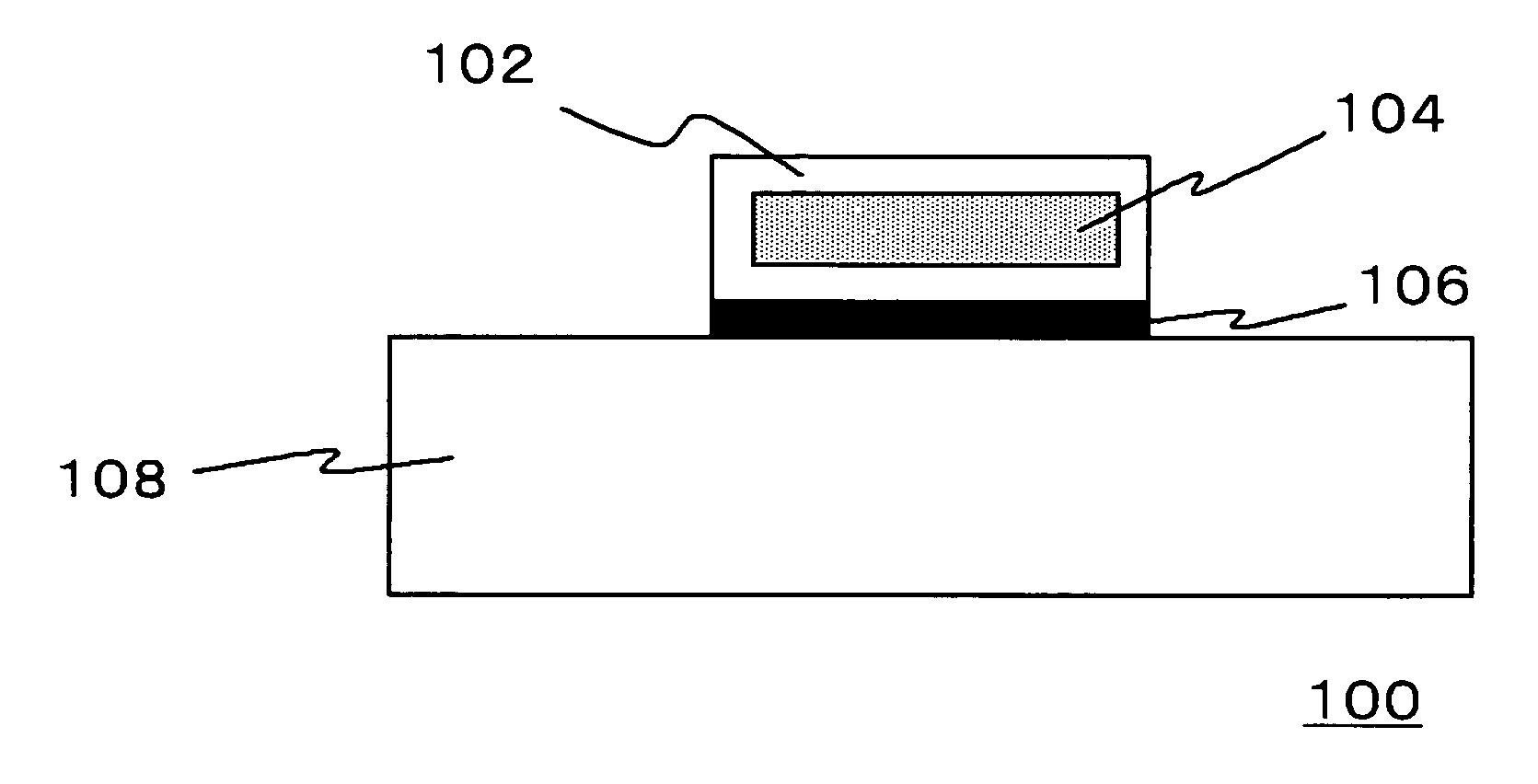
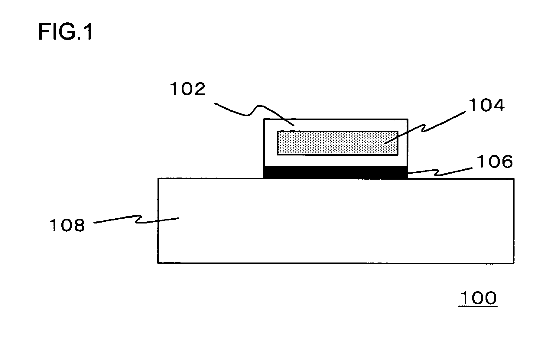
[0042]FIG. 1 is a schematic cross-sectional diagram which shows a gate structure of a solid state imaging device according to the present embodiment. A gate structure 100 according to the present embodiment includes: a silicon substrate 108; a silicon oxide film 106 formed on the silicon substrate 108; and a polysilicon film 104 formed on the silicon oxide film 106. Each of the upper face, the bottom face, and both side faces, of the polysilicon film 104 are coated with a silicon nitride film 102.
[0043] The polysilicon film 104 serves as a transfer electrode of the solid state imaging device. The silicon nitride film 102 serves as an insulating coating film for coating the bottom face, the upper face, and both side faces, of the transfer electrode. The silicon oxide film 106 serves as a gate insulating film. The silicon substrate 108 serves as a semiconductor substrate. The gate structure 100 including the aforementioned components forms a transfer portion of the solid state imagin...
second embodiment
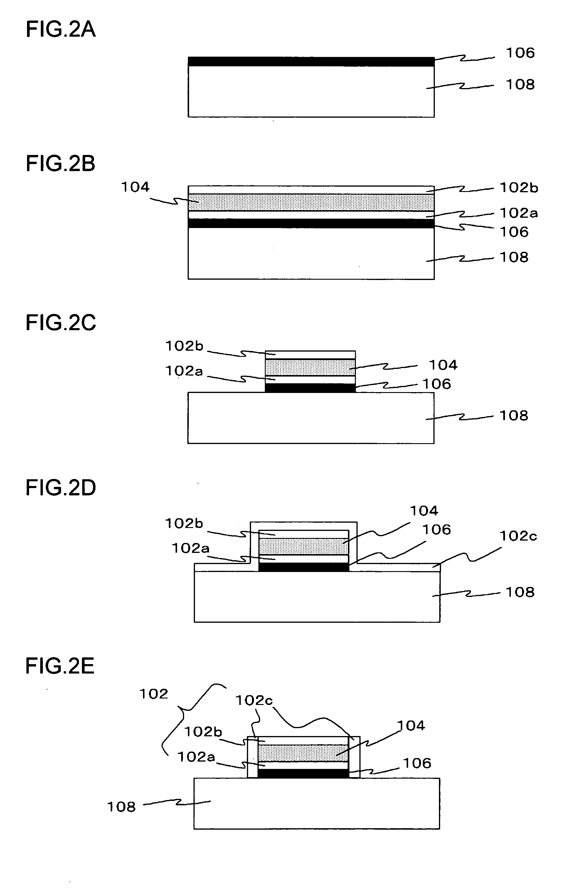
[0091]FIGS. 2A through 2E are a series of cross-sectional diagrams, which shows an example of the gate structure of the solid state imaging device according to the present embodiment for each manufacturing step. The gate structure of the solid state imaging device according to the present embodiment may be formed with a manufacturing method according to the present embodiment shown in FIG. 2, wherein, following formation of the three-layer structure including the transfer electrodes, side-wall formation is performed.
[0092] Specifically, as shown in FIG. 2A, first, the silicon oxide film 106 is layered on the silicon substrate 108. Subsequently, as shown in FIG. 2B, the silicon nitride film 102a, the polysilicon film 104, and the silicon nitride film 102b, are layered on the silicon oxide film 106 in that order.
[0093] Subsequently, a resist film (not shown) is formed on the silicon nitride film 102b, and patterning of the resist film is performed. Then, as shown in FIG. 2C, etching...
third embodiment
[0100]FIG. 9 is a cross-sectional diagram which shows an modification of a gate structure of a solid state imaging device according to the present embodiment. A gate structure 400 of the solid state imaging device according to the present embodiment includes a silicon nitride film 102a formed on the silicon substrate 108, the polysilicon film 104 formed on the silicon nitride film 102a, and a silicon nitride film 102d for coating the upper face and both side faces of the polysilicon film 104.
[0101] With such a structure, the bottom face, the upper face, and both side faces of the polysilicon film 104 are coated with the silicon nitride films 102a and 102d, as well. Thus, such a gate structure prevents erosion of both side faces of the polysilicon film 104 due to infiltration of an etchant at the time of etching processing for other components. Thus, such a gate structure suppresses increase of the resistance of the polysilicon film 104.
[0102] Furthermore, the silicon nitride films...
PUM
 Abstract
Description
Claims
Application Information
 - R&D
- Intellectual Property
- Life Sciences
- Materials
- Tech Scout
- Unparalleled Data Quality
- Higher Quality Content
- 60% Fewer Hallucinations
Browse by: Latest US Patents, China's latest patents, Technical Efficacy Thesaurus, Application Domain, Technology Topic, Popular Technical Reports.
© 2025 PatSnap. All rights reserved.Legal|Privacy policy|Modern Slavery Act Transparency Statement|Sitemap|About US| Contact US: help@patsnap.com