Semiconductor device including gate electrode for applying tensile stress to silicon substrate, and method of manufacturing the same

a technology of tensile stress and silicon substrate, which is applied in the direction of semiconductors, semiconductor devices, electrical equipment, etc., can solve the problems of inapplicability to sti, insufficient activation annealing, and large number of problems to be solved, so as to improve carrier mobility and simplify manufacturing steps

Inactive Publication Date: 2005-09-15
RENESAS ELECTRONICS CORP
View PDF6 Cites 6 Cited by
  • Summary
  • Abstract
  • Description
  • Claims
  • Application Information

AI Technical Summary

Benefits of technology

[0013] It is therefore an object of the present invention to provide a semiconductor device allowing improvement in carrier mobility by applying tensile stress only to a channel region of a desired MOS transistor, and allowing simplification of manufacturing steps. It is still an object of the present invention to provide a method of this semiconductor device.
[0015] Tensile stress is applied to a region in the silicon substrate defined under a predetermined gate electrode. Therefore, lattice spacing is widened in this region of the silicon substrate. When this gate electrode is applied to an nMOS transistor, for example, enhancement of carrier mobility can be provided, thus contributing to performance improvement of the nMOS transistor.
[0017] Compressive residual stress is exerted on a predetermined gate electrode as internal stress therein, to apply tensile stress to a region in the silicon substrate defined under the gate electrode. Therefore, lattice spacing is widened in this region of the silicon substrate. When this gate electrode is applied to an NMOS transistor, for example, enhancement of carrier mobility can be provided, thus contributing to performance improvement of the NMOS transistor. Further, a mass number of ion to be implanted may vary according to the type of the gate electrode, or a part of the predetermined film on the predetermined gate electrode may be removed prior to thermal processing. Therefore, even when a plurality of gate electrodes are formed in the same step, only a desired gate electrode can easily be subjected to high compressive stress exerted thereon. As a result, simplification of the manufacturing steps is provided.

Problems solved by technology

On the other hand, the strained silicon substrate encounters the problems as follows which result from use of SiGe as a substrate material: crystal defect and deterioration in surface roughness caused by SiGe, rise in substrate temperature due to low heat conductivity of SiGe, increase in short-channel effect in a p-channel MOS transistor covering band discontinuity at an interface between SiGe and Si, or the like.
Other problems involved therein associated with process steps include inapplicability to STI (shallow trench isolation) technique, or insufficient activation annealing, for example.
In view of this, for actually using the strained silicon substrate in LSIs, there remain a lot of problems to be solved.
As a result, a gate electrode of the nMOS transistor and that of the pMOS transistor cannot be provided in the same process step, causing complication of the manufacturing steps.

Method used


Image

  • Semiconductor device including gate electrode for applying tensile stress to silicon substrate, and method of manufacturing the same
  • Semiconductor device including gate electrode for applying tensile stress to silicon substrate, and method of manufacturing the same
  • Semiconductor device including gate electrode for applying tensile stress to silicon substrate, and method of manufacturing the same

Examples


first preferred embodiment

[0026] The present inventors have found that when amorphous silicon including a large number of ions implanted therein undergoes thermal processing to form recrystallized polycrystalline silicon (polysilicon), volume expansion of silicon occurs. It has also been found that the amount of expansion of silicon is controlled largely by the mass number of ions implanted therein, and more particularly, that the amount of expansion increases as the mass number of implanted ions becomes larger (more specifically, 70 or more). It has been confirmed as well that the amount of expansion increases as the implant dose of ions increases.

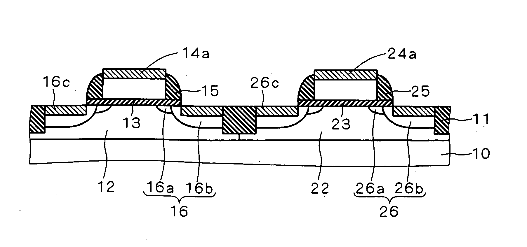
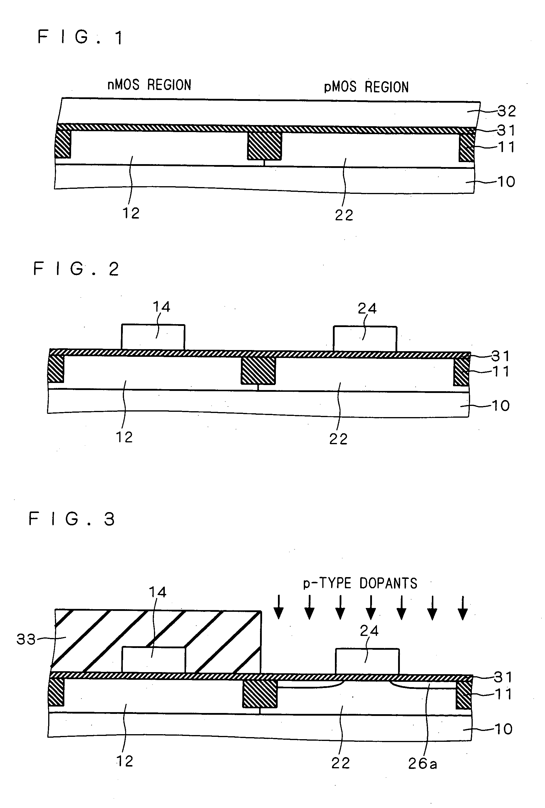
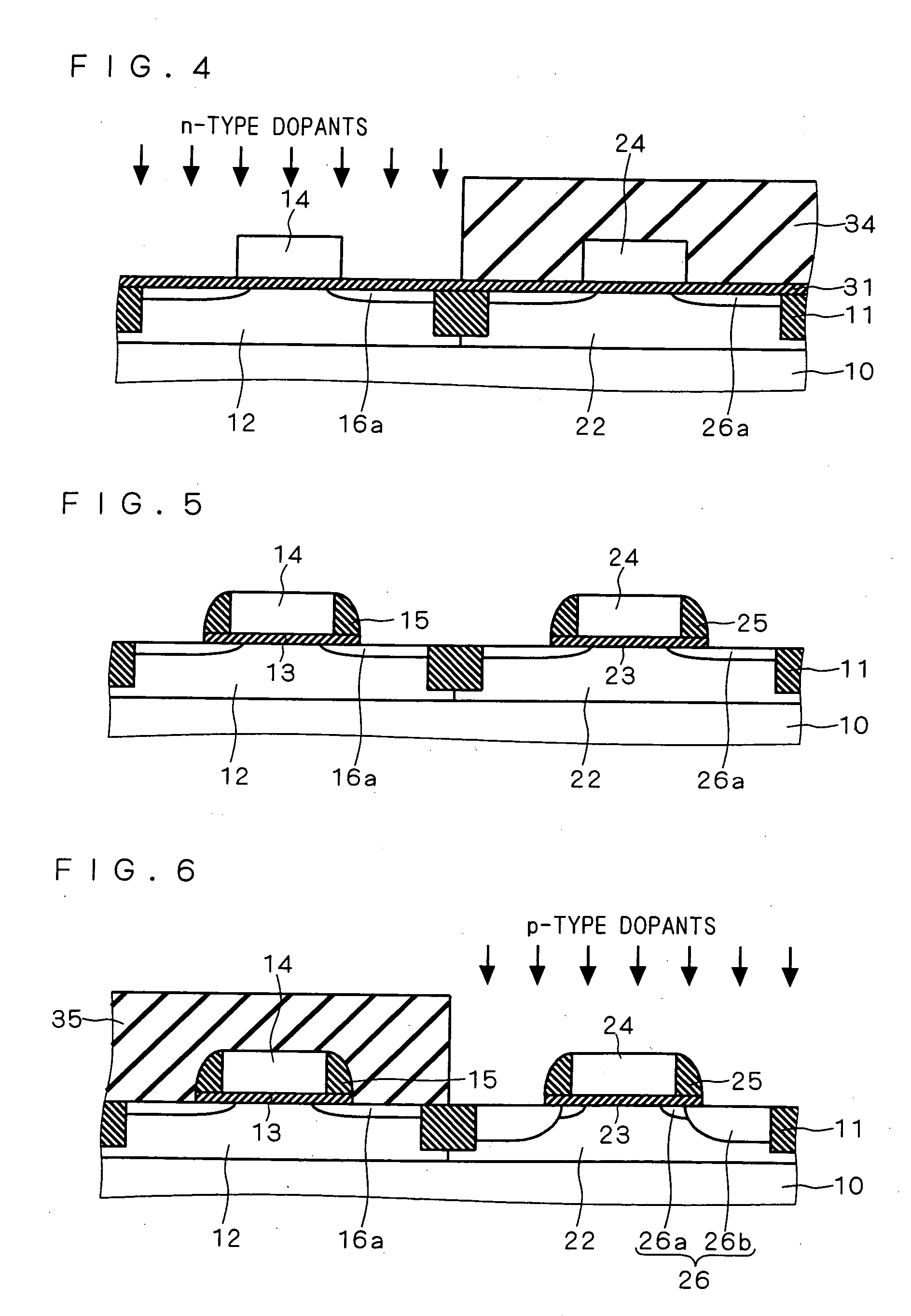
[0027]FIGS. 1 through 9 illustrate steps of manufacturing a semiconductor device according to the first preferred embodiment of the present invention. In each one of FIGS. 1 through 9, the left half shows a region for forming an NMOS transistor (hereinafter called as an “nMOS region”), and the right half shows a region for forming a pMOS transistor (hereinafter c...

second preferred embodiment

[0048] As discussed in the first preferred embodiment, ions having a relatively small mass number are implanted into the gate electrode 24, and therefore, there will be little residual stress to be applied to the gate electrode 24 even with the existence of the silicon oxide film 40 thereon. In the case of ion implantation in large quantity, however, there may be some compressive residual stress to be exerted on the gate electrode 24 even when the implanted ions have a small mass number.

[0049] The steps of manufacturing a semiconductor device according to the second preferred embodiment of the present invention will be given. First, following the same steps as those of the first preferred embodiment shown in FIGS. 1 through 8, the NMOS and pMOS transistors are provided. Further provided thereon is the silicon oxide film 40. Next, the silicon oxide film 40 in the pMOS region is removed so that an opening is defined therein, as shown in FIG. 11.

[0050] Thermal processing is thereafte...

third preferred embodiment

[0053] In the first and second preferred embodiments, ion implantation for forming the n-type source / drain diffusion layer 16b is also operative to implant ions into the gate electrode 14 for expansion thereof. Alternatively, ion implantation step into the gate electrode 14 may be performed separately from the implantation step for formation of the n-type source / drain diffusion layer 16b.

[0054] The steps of manufacturing a semiconductor device according to the third preferred embodiment of the present invention will be given. First, following the same steps as those of the first preferred embodiment shown in FIGS. 1 through 6, the nMOS and pMOS transistors are provided. Next, a resist mask 36 is formed to have an opening in the pMOS region. Thereafter, prior to formation of the n-type source / drain diffusion layer 16b in the NMOS region, electrically inactive ions having a relatively large mass number (70 or more) such as Ge ions are entirely implanted with a dose of 4×10¹⁵ / cm2 or m...


PUM


Abstract

A gate insulating film (13) and a gate electrode (14) of non-single crystalline silicon for forming an NMOS transistor are provided on a silicon substrate (10). Using the gate electrode (14) as a mask, n-type dopants having a relatively large mass number (70 or more) such as As ions or Sb ions are implanted, to form a source / drain region of the NMOS transistor, whereby the gate electrode (14) is amorphized. Subsequently, a silicon oxide film (40) is provided to cover the gate electrode (14), at a temperature which is less than the one at which recrystallization of the gate electrode (14) occurs. Thereafter, thermal processing is performed at a temperature of about 1000° C., whereby high compressive residual stress is exerted on the gate electrode (14), and high tensile stress is applied to a channel region under the gate electrode (14). As a result, carrier mobility of the NMOS transistor is enhanced.

Description

BACKGROUND OF THE INVENTION [0001] 1. Field of the Invention [0002] The present invention relates to a semiconductor including a MOS (metal oxide semiconductor) field effect transistor, and method of manufacturing the same. [0003] 2. Description of the Background Art [0004] For a MOS field effect transistor (MOS transistor), increase in drain current as a driving current is one of the ways of improving characteristic of this MOS transistor. Carrier mobility is one of the determinants of drain current. The carrier mobility is virtually controlled by a substrate material, and therefore, it can hardly be changed. On the other hand, it has been found that scattering probability and effective mass of carriers are altered by the change in lattice spacing of substrate atoms, allowing change of carrier mobility. [0005] SiGe has wider lattice spacing than Si. In a substrate including SiGe and Si stacked thereon, the lattice spacing of the upper-layer Si is widened accordingly. The substrate ...

Claims


Application Information

Patent Timeline
Patent Type & Authority Applications(United States)
IPC IPC(8): H01L21/265H01L21/28H01L21/336H01L21/8234H01L21/8238H01L27/088H01L27/092H01L29/423H01L29/49H01L29/78
CPCH01L21/26506H01L21/32155H01L21/823807H01L21/823814H01L21/823828H01L21/823842H01L27/1104H01L29/7842H01L29/7845H01L21/823412H01L29/66477H01L27/10844H01L29/665H10B12/01H10B10/12H01L29/78H10B10/18H10B12/09H10B12/30H10B12/50H01L29/4925H01L21/823418H01L21/823443H01L29/4933H01L21/823835H01L29/7848
Inventor SAYAMA, HIROKAZUOHTA, KAZUNOBUODA, HIDEKAZUSUGIHARA, KOUHEI
Owner RENESAS ELECTRONICS CORP
Why Eureka
Try Eureka