Semiconductor apparatus

a technology of semiconductor devices and components, applied in the direction of cross-talk/noise/interference reduction, non-metallic protective coating applications, and improvement of metal adhesion of the insulating substrate, can solve the problems of drop in the yield of element fabrication processes, and poor reliability of elements, and achieve excellent interface adhesion

Inactive Publication Date: 2005-09-22
SANYO ELECTRIC CO LTD
View PDF9 Cites 35 Cited by
  • Summary
  • Abstract
  • Description
  • Claims
  • Application Information

AI Technical Summary

Benefits of technology

[0022] Also, the substrate is generic to a semiconductor chip, a semiconductor wafer and a resin film formed on a substrate. More specifically, according to the present invention, the top surface of the substrate may be brought into contact with the surfaces of the elements or the semiconductor chips subjected to plasma treatment. Alternatively, the top surface of a protective film provided on the uppermost layer of the substrate may be brought into contact with the surfaces of the elements or the semiconductor chips subjected to plasma treatment. The elements are generic to semiconductor elements such as semiconductor chips, and passive elements such as resistors, capacitors and conductors. In plasma treatment, a plasma gas including an inactive gas is preferably used. With this, degradation in the performance of substrate is controlled and the surface providing excellent interface adhesion is obtained.

Problems solved by technology

When semiconductor chips are build in layers, however, satisfactory adhesion between the semiconductor chips built in layers is not ensured, causing the reliability of elements to become poor and the yield in element fabrication process to drop.
When adhesion at the interface is poor, the elements are affected by thermal stress and humidity, causing the reliability of elements to become poor.

Method used


Image

  • Semiconductor apparatus
  • Semiconductor apparatus
  • Semiconductor apparatus

Examples


first embodiment

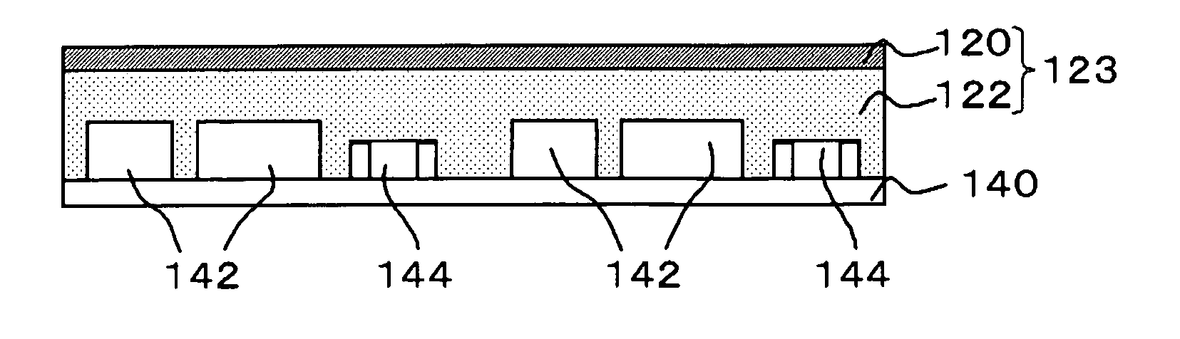
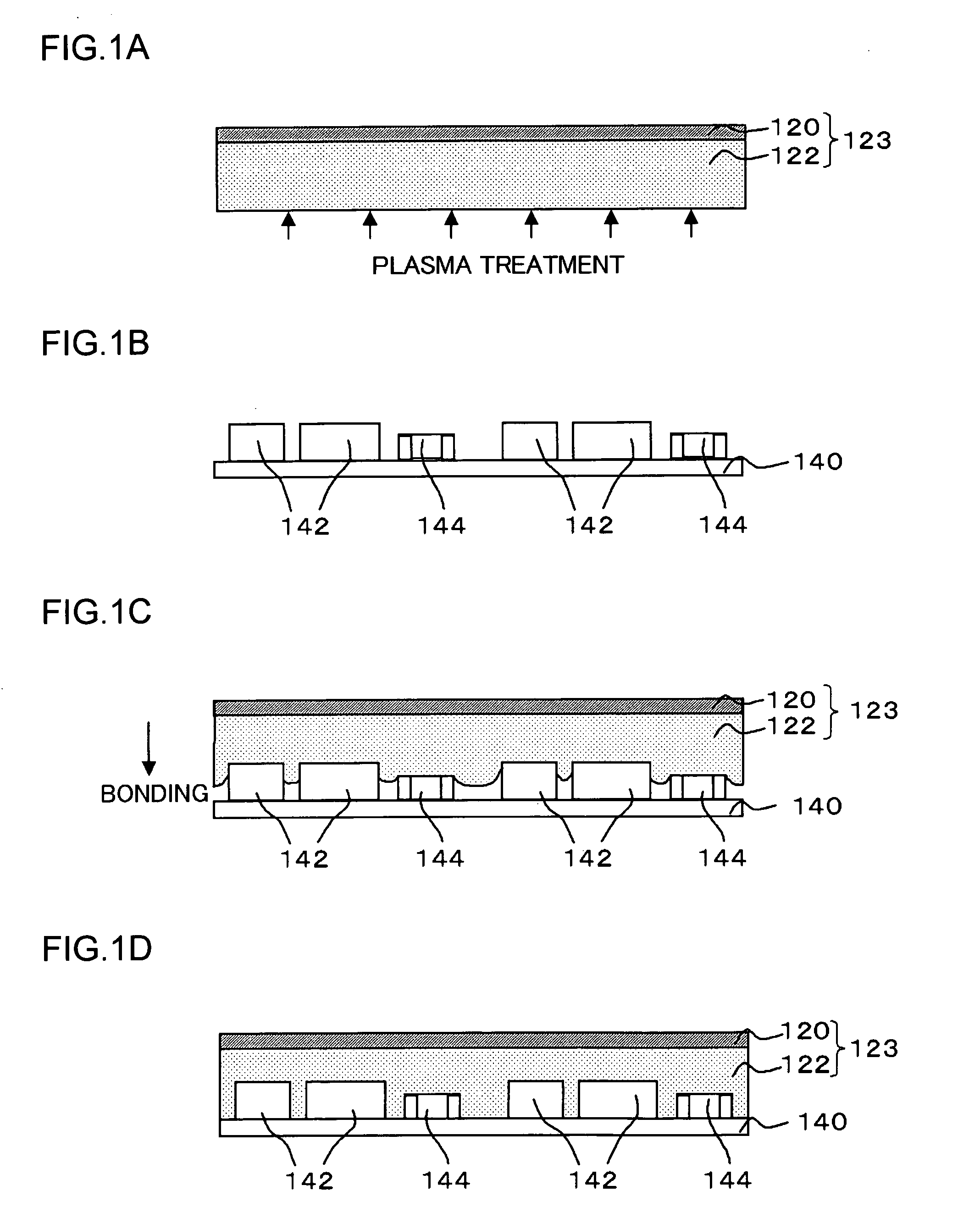
[0038]FIGS. 1A-1D are sections illustrating a process of fabricating a semiconductor apparatus according to a first embodiment of the present invention. As shown in FIG. 1A, the bottom surface of a composite of conductive film and resin insulating film 123 comprising a conductive film 120 and a resin insulating film 122 is plasma treated. The conductive film 120 may be a rolled metal such as a rolled copper foil. Any material may be used to form the resin insulating film 122 as long as it is softened by heating. For example, epoxy resin, melamine derivatives such as BT resin, liquid crystal polymer, PPE resin, polyimide resin, fluororesin, phenol resin, polyamide bismaleimide may be used. In addition to the resin, a filler or an additive such as SiO2 may be added as appropriate.

[0039] The plasma irradiation condition is set to adapt to the resin material used so that surface properties superior in interface adhesion are obtained. For example, the condition may be established such t...

second embodiment

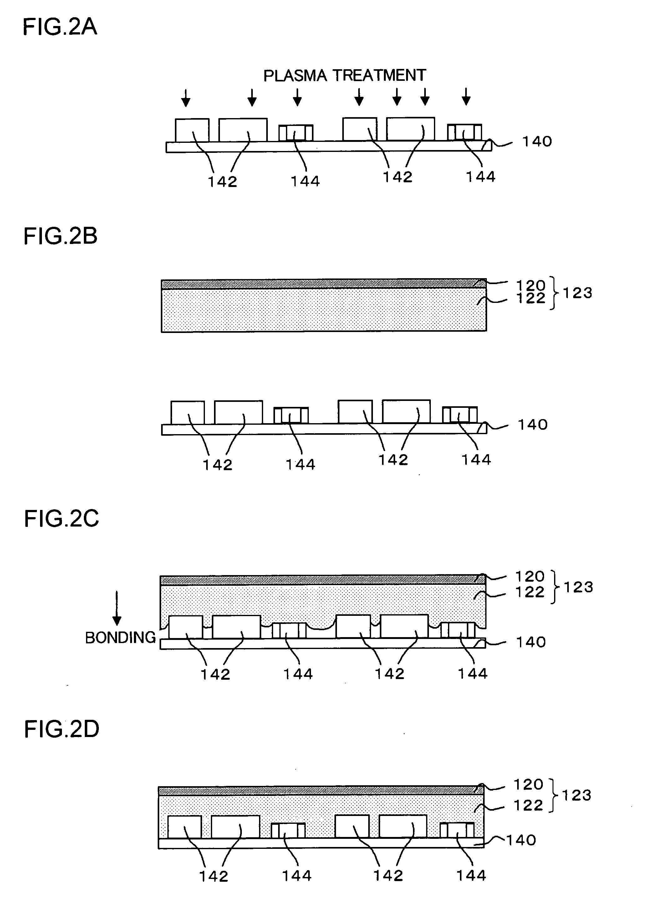
[0050] In the first embodiment, the bottom surface of the resin insulating film 122 is described as being plasma treated. In a second embodiment according to the present invention, a description will be given of the structure in which the top surface of each of the substrate 140, the semiconductor elements 142 and the passive elements 144 is plasma treated.

[0051] As shown in FIG. 2A, the top surface of each of the substrate 140, and the circuit elements, including the plurality of semiconductor elements 142 and the plurality of passive elements 144 fixed on the substrate 140 is plasma treated. The plasma irradiation condition is set to adapt to the resin material used so that surface properties superior in interface adhesion are obtained. For example, the condition may be established such that an inactive gas like argon is included in a plasma gas so as to improve the efficiency with which organic substance, collected on the top surface of the circuit elements including the plurali...

third embodiment

[0062] Unlike the first embodiment and the second embodiment, a third embodiment of the present invention uses an elastic material as the substrate 140. A PET film, polypropylene (PP), polyamide (PA), polyethylen (PE) may be used to form the substrate 140 according to the third embodiment.

[0063]FIGS. 3A-3C are sections illustrating a process of fabricating a semiconductor apparatus according to the third embodiment. As shown in FIG. 3A, after fixing the plurality of semiconductor elements 142 and the plurality of passive elements 144 on the substrate 140, the substrate 140 is extended horizontally as illustrated. The substrate 140 is extended by clamping the ends of the substrate 140 by a fastening device and extending the substrate 140 horizontally as illustrated. As shown in FIG. 3B, the composite of conductive film and resin insulating film 123 plasma treated in a condition similar to that of the first embodiment is placed on the substrate 140, in a state in which the substrate ...


PUM


Abstract

A semiconductor apparatus includes a substrate and elements or semiconductor chips provided on the substrate. The elements are sealed by being brought into contact with a sealing compound. The surface of contact on the elements or the sealing compound is plasma treated. The semiconductor chip is adhesively attached to another semiconductor chip via an adhesive compound. The surface of the semiconductor chip in contact with the adhesive compound is plasma treated.

Description

BACKGROUND OF THE INVENTION [0001] 1. Field of the Invention [0002] The present invention relates to a semiconductor apparatus on which elements or semiconductor chips are mounted, and also relates to a method of fabricating the apparatus. [0003] 2. Description of the Related Art [0004] With portable electronic appliances such as mobile phones, PDAs, DVCs and DSCs becoming more and more advanced in their capabilities, miniaturization and weight reduction of products have become essential for market acceptance. Accordingly, highly-integrated system LSIs for achieving these goals are demanded. Also, better ease and convenience of use are required of these electronic appliances. In this respect, high capabilities and high performance are required of LSIs used in these appliances. While the number of I / Os is increasing as a result of increasingly high integration of LSI chips, there is also a persistent requirement for miniaturization of packages themselves. In order to meet these incom...

Claims


Application Information

Patent Timeline
Patent Type & Authority Applications(United States)
IPC IPC(8): H01L21/56H01L23/31H01L23/48H01L25/16H05K1/02H05K3/28H05K3/38
CPCH01L21/56H01L23/3128H01L24/48H05K2203/1311H05K2203/095H05K3/381H05K3/284H05K1/0218H01L2924/19105H01L23/3142H01L25/16H01L2224/16225H01L2224/32145H01L2224/32225H01L2224/48091H01L2224/48145H01L2224/48227H01L2224/48465H01L2224/73204H01L2224/73265H01L2924/15311H01L2924/19041H01L2924/00014H01L2924/00012H01L2924/00H01L24/45H01L24/73H01L2224/451H01L2924/181H01L2924/00015H01L2224/05599
Inventor USUI, RYOSUKENISHIDA, ATSUHIROMIZUHARA, HIDEKINAKAMURA, TAKESHI
Owner SANYO ELECTRIC CO LTD
Why Eureka
Try Eureka