Low noise op amp

a low-noise op amp and low-noise technology, applied in the field of amplifiers, can solve the problems of flicker noise improvement and over-all flicker noise of the circuit, and achieve the effects of reducing oxide thickness, low operating voltage, and reducing flicker nois

Active Publication Date: 2005-09-22
CIRRUS LOGIC INC
View PDF10 Cites 18 Cited by
  • Summary
  • Abstract
  • Description
  • Claims
  • Application Information

AI Technical Summary

Benefits of technology

[0016] In general terms the present invention provides an analogue circuit arrangement using MOS based technology which reduces flicker noise by reducing the oxide thickness of selected transistor devices, having a low operating voltage, compared with those required to operate with a larger operating voltage in the same circuit. The lower voltage transistors are typically employed for biasing, constant current sources, and current mirrors, whereas the larger voltage transistors are exposed to the necessary large signal swings for hi fidelity audio operation. The reduced oxide thickness reduces the flicker noise contribution to the circuit from these low voltage transistors, and hence the overall flicker noise of the circuit. The cascode transistor(s) will still require a thicker oxide layer in order to handle the higher voltage level, whereas the other circuit transistors can be implemented with thinner oxide layers by arranging the circuit such that they are only required to handle relatively low operating voltages.
[0017] Advantageously, this dual transistor oxide thickness arrangement can be utilised in a folded cascode op amp circuit in which the transistors required to handle the larger voltages are the cascode transistors, which because of the nature of cascode circuits have a much reduced flicker noise contribution compared with transistors in other circuit configurations. Thus a number of the non-cascode circuit transistors can have thinner oxide layers in order to further minimise their contributions to the flicker noise of the op amp circuit.
[0018] A further advantage of this arrangement is that the overall chip size can be reduced because of the replacement of thicker oxide layer transistors by thinner oxide transistors. For a given width and length and operating current and voltage, the thinner gate oxide transistor will have high transconductance and higher output impedance: conversely for a given requirement for transconductance or output impedance, the width and length can be scaled, giving a smaller chip area occupied by the transistor. Of course this scaling will also reduce the improvement in flicker noise, but this is a tradeoff available to the designer.
[0022] Preferably the second transistor device forms part of a cascode transistor device circuit within said analogue circuit. Preferably the cascode transistor device circuit is a differential folded cascode op amp circuit. This reduces the flicker noise contribution of the thicker oxide layer transistors.

Problems solved by technology

The reduced oxide thickness reduces the flicker noise contribution to the circuit from these low voltage transistors, and hence the overall flicker noise of the circuit.
Of course this scaling will also reduce the improvement in flicker noise, but this is a tradeoff available to the designer.

Method used


Image

  • Low noise op amp
  • Low noise op amp
  • Low noise op amp

Examples


Embodiment Construction

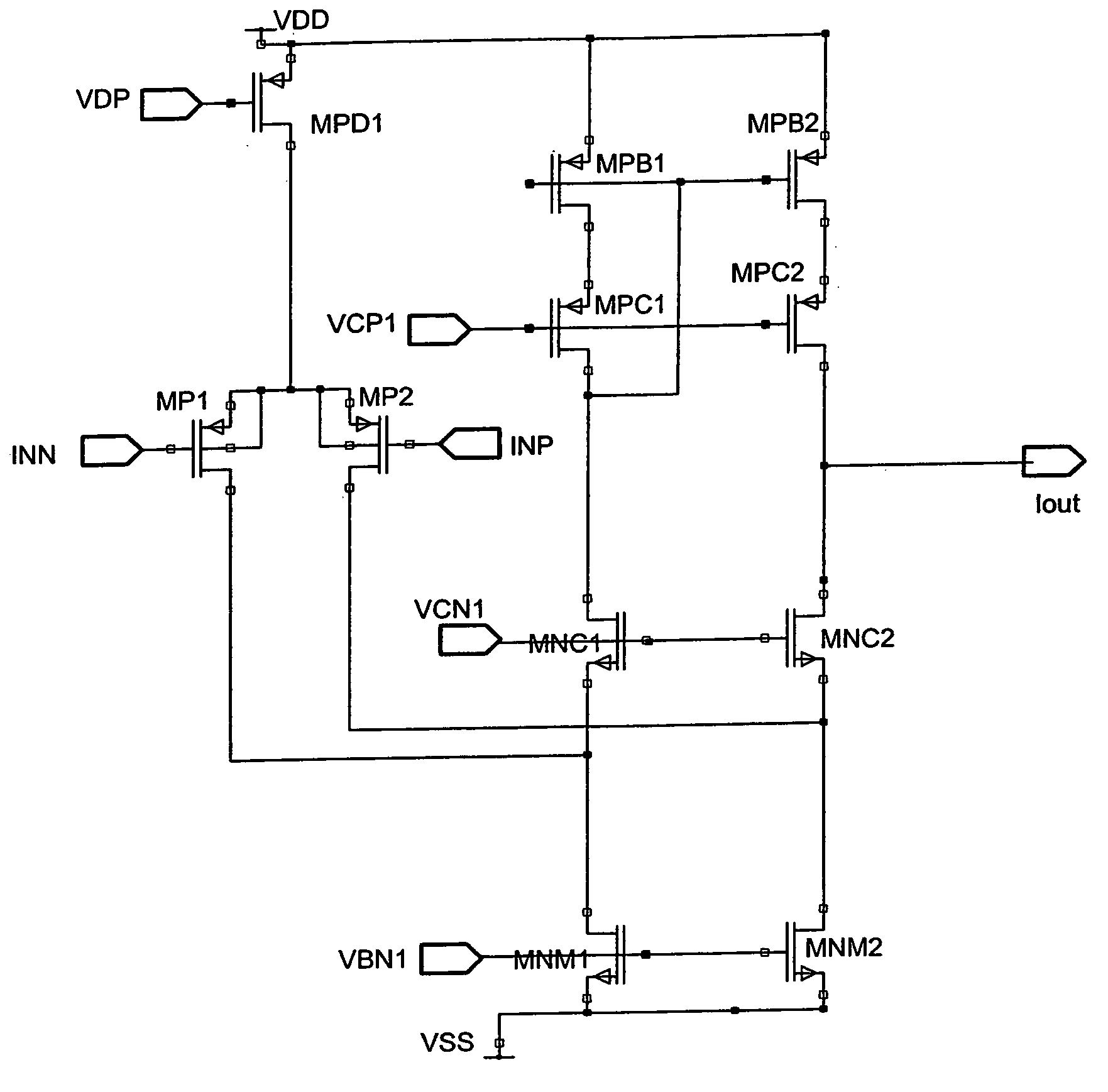
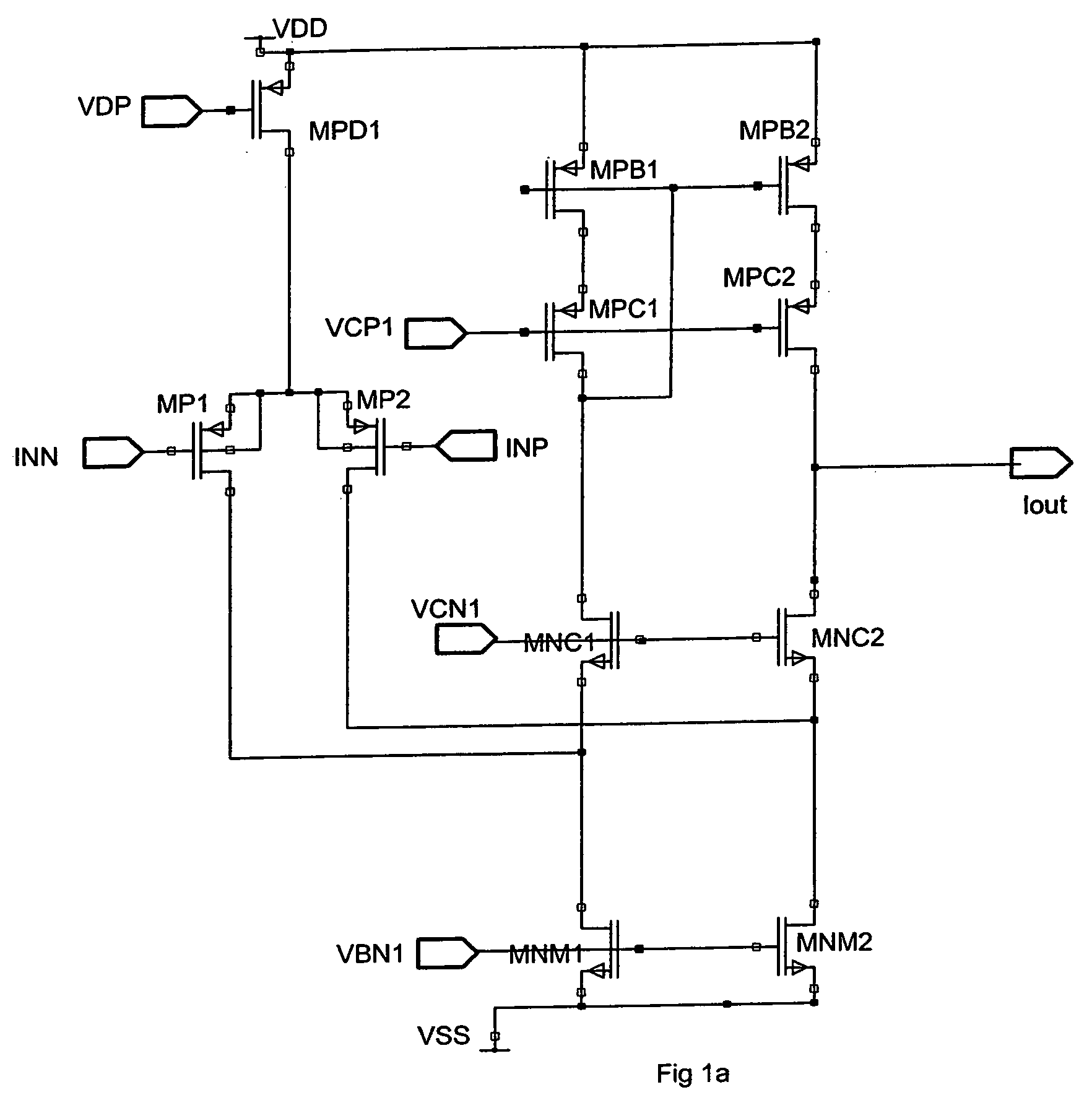
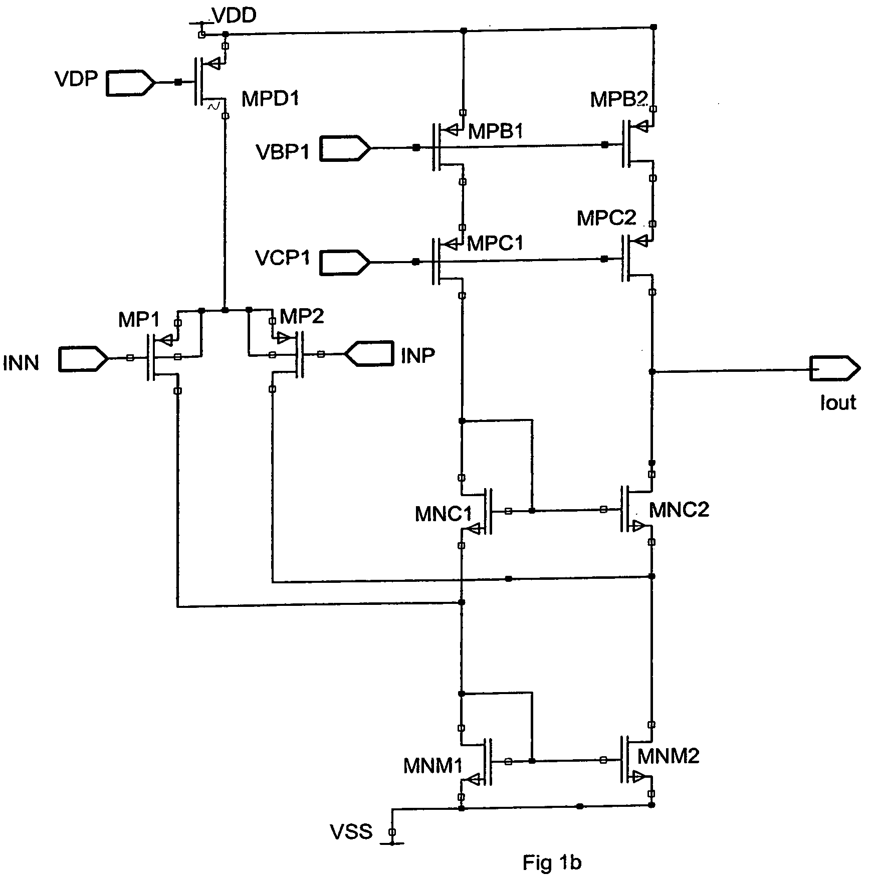
[0037] Referring initially to FIG. 1b, a typical audio op amp design is shown which utilises a differential folded cascode arrangement. MOS based transistor devices MP1 and MP2 are input transistors. Signal current from MP2 passes through folded cascode device MNC2 to the output. Signal current from MP1 cannot pass through folded cascode device MNC1, since current I(MNC1) is equal to the constant current defined by the constant current source MPB1. The MP1 signal current therefore passes through the current mirror formed by MNM1, MNM2 and then through the cascode device MNC2 to the output. Thus MNM1, MNM2, MNC1, MNC2 act as a single ended to differential converter, as well as contributing a cascode function to increase output impedance of this transconductance stage. Transistors MPC1 and MPC2 serve as cascode devices to bias devices MPB1 and MPB2 to increase their effective output impedance, to maintain the high output impedance at Iout and also to improve power supply rejection.

[0...


PUM


Abstract

The present invention relates amplifiers using metal oxide semiconductor based integrated circuits. The present invention is particularly but not exclusively related to audio application mixed signal chips. The present invention provides an analogue circuit for processing analogue signals in an integrated circuit comprising a number of metal oxide semiconductor transistor devices, the circuit stage comprising a first said transistor device having a first oxide thickness, and a second said transistor device having a second and different oxide thickness. Preferably a cascode based op amp structure is implemented.

Description

FIELD OF THE INVENTION [0001] The present invention relates to amplifiers using metal oxide semiconductor based integrated circuits. The present invention is particularly but not exclusively related to audio application mixed signal chips. BACKGROUND OF THE INVENTION [0002] Due to the increasing need for miniaturisation of portable devices such as MP3 players, mobile telephones and personal digital assistants, it has become increasingly important to implement both digital processing functions and related analogue, especially audio, processing functions on the same chip or integrated circuit—a so called mixed signal chip. For this reason the implementation of analogue functions on metal oxide semiconductor (MOS) based devices has become increasingly important. [0003] A major problem with this technology however is that the digital and analogue circuits require different characteristics from the same semiconductor technology. Digital circuits are fastest and consume least power and ch...

Claims


Application Information

Patent Timeline
Patent Type & Authority Applications(United States)
IPC IPC(8): H03F1/22H03F1/26H03F1/52H03F3/16H03F3/45
CPCH03F1/26H03F3/187H03F2203/45674H03F3/45192H03F3/45183
Inventor RICHARD, PATRICK E.PENNOCK, JOHN L.
Owner CIRRUS LOGIC INC
Why Eureka
Try Eureka