

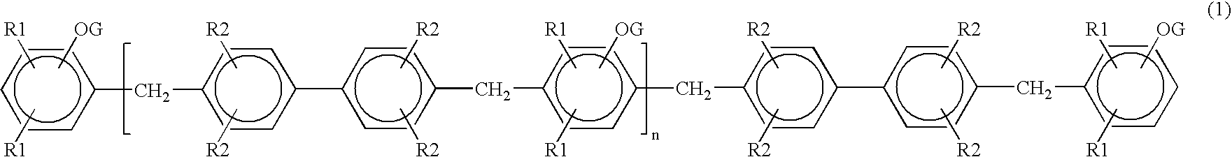
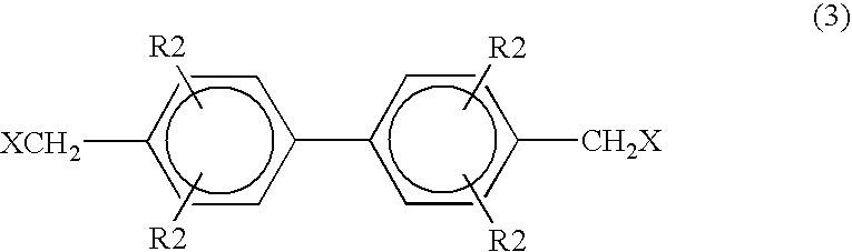
Epoxy resin composition and semiconductor device
a technology of epoxy resin and semiconductor device, which is applied in the direction of synthetic resin layered products, semiconductor/solid-state device details, transportation and packaging, etc., can solve the problems of poor adhesion properties of palladium plating, increase cracks in resin, and difficult to ensure the reliability of semiconductor device, etc., to achieve excellent flame retardance, excellent reliability and productivity
- Summary
- Abstract
- Description
- Claims
- Application Information
AI Technical Summary
Benefits of technology
Problems solved by technology
Method used
Image


Examples
experimental example 1
[0068] Epoxy resin E-1: 76.2 parts by weight
[0069] Phenolic resin H-1: 51.0 parts by weight
[0070] Triphenylphosphine: 1.8 parts by weight
[0071] Spherical fused silica powder (average particle size: 16.0 μm, maximum particle size: 75 μm): 860.0 parts by weight
[0072]γ-Glycidoxypropyltrimethoxysilane: 4.0 parts by weight
[0073] Carnauba wax: 4.0 parts by weight
[0074] Carbon black: 3.0 parts by weight
[0075] All of these components were blended in a mixer and the mixture was kneaded 30 times using two rolls with surface temperatures of 90° C. and 45° C. to obtain the kneaded product sheet. The kneaded product sheet was cooled and then pulverized to give a resin composition. The resin composition was evaluated for its properties as follows. The evaluation results are shown in Table 1.
Evaluation and analyses
[0076] GPC analyzer [0077] Liquid feeding pump L-6000 (Hitachi, Ltd.) [0078] UV detector: L-4000 (Hitachi, Ltd.) [0079] Determined as an absorbance at 254 nm [0080] Column: KF-...
experimental examples 2 to 13
[0101] With the formulations shown in Table 1, molding materials were prepared as described in Experimental example 1. Using these molding materials, evaluation was conducted as described in Experimental example 1. The evaluation results are shown in Table 1.
TABLE 1Experimental ExamplesFormulation (parts by weight)12345678910111213E-1 76.2 76.0 73.0 77.0 38.6 76.2 76.2 76.2 76.0 80.5 94.6E-2 18.3 55.9E-3 9.6 65.4H-1 51.0 65.7 25.5H-2 51.2 40.2 23.5H-3 51.0 51.3H-4 25.5 51.0 61.8H-5 51.2H-6 10.1 46.7H-7 5.9 32.6Triphenylphosphine 1.8 1.8 2.0 1.8 1.4 1.8 1.8 1.8 1.8 1.8 1.8 1.8 1.8Spherical fused silica powder860.0860.0830.0860.0910.0860.0860.0860.0860.0880.0860.0860.0860.0γ-glycidoxypropyltrimethoxysilane 4.0 4.0 4.0 4.0 4.0 4.0 4.0 4.0 4.0 4.0 4.0 4.0 4.0Carnauba wax 4.0 4.0 4.0 4.0 4.0 4.0 4.0 4.0 4.0 4.0 4.0 4.0 4.0Carbon black 3.0 3.0 3.0 3.0 3.0 3.0 3.0 3.0 3.0 3.0 3.0 3.0 3.0Spiral flowcm130 125 170 123 85 128 132 135 131 92 100 90 102 Soldering heat resistanc...
PUM
| Property | Measurement | Unit |
|---|---|---|
| temperature | aaaaa | aaaaa |
| softening point | aaaaa | aaaaa |
| softening point | aaaaa | aaaaa |
Abstract
Description
Claims
Application Information